Home > Press > The world's sharpest X-ray beam shines at DESY: Researchers of the University of Gottingen substantially increase resolution at DESY's light source PETRA III
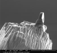 |
| This is an electron micrograph of the micro lens on the tip of a needle. The lens has a diameter of just two microns (thousandths of a millimeter).
Credit: Image: University of Göttingen |
Abstract:
The world's sharpest X-ray beam shines at DESY. At the X-ray light source PETRA III, scientists from Göttingen generated a beam with a diameter of barely 5 nanometres - this is ten thousand times thinner than a human hair. This fine beam of X-ray light allows focusing on smallest details. The research groups of Professor Tim Salditt from the Institute of X-ray Physics and of Professor Hans-Ulrich Krebs from the Institute of Materials Physics of the University of Göttingen published their work in the research journal Optics Express.
The world's sharpest X-ray beam shines at DESY: Researchers of the University of Gottingen substantially increase resolution at DESY's light source PETRA III
Göttingen, Germany | Posted on September 30th, 2013High-energy (hard) X-ray light cannot be focused as easily as visible light by using a burning glass. "Instead of a common lens, we use a so-called Fresnel lens which consists of several layers," explains co-author Dr. Markus Osterhoff. The central support is a fine tungsten wire with the thickness of only a thousandth of a millimetre. Around the wire, nanometre-thin silicon and tungsten layers are applied in an alternating way. The physicists then cut a thin slice from the coated wire. "This slice has 50 to 60 silicon and tungsten layers, comparable to growth rings of a tree," explains team member Florian Döring. "And the layer thicknesses have to be extremely precise," adds Christian Eberl. The two PhD students have optimized the different fabrication steps.
The wire slice with a size of only about two thousandths of a millimetre is used as a lens. However, it does not diffract light like a glass lens but scatters it like an optical grid generating a pattern of bright and dark patches. In this case, the thickness of the layers is selected in such a way that the bright areas of the diffraction pattern coincide at the same spot. The more precise the lens is fabricated, the sharper becomes the X-ray focus. With this method, the physicists obtained an X-ray beam of 4.3 nanometres (millionth of a millimetre) diameter in horizontal direction and 4.7 nanometres diameter in vertical direction. Until recently it was even debated whether fundamental limits of X-ray optics would stand against such small focal widths. The outstanding brilliance of DESY's X-ray light source PETRA III helped to make a usable nano focus possible.
The fine X-ray beam opens up new possibilities for materials science, e.g. the investigation of nano wires to be used in solar cells. "Usually, when investigating the chemical composition of a sample, the beam size limits the sharpness of the image. Before this experiment, this limit was at about 20 nanometers", said DESY researcher Dr. Michael Sprung, responsible scientist for the PETRA measuring station P10, where the experiments are carried out.
As a next step, the scientists want to improve the performance by depositing the layers on ultrathin and extremely uniform glass fibres. Moreover, they plan to scan first nanoscopic structures with their novel ultra-sharp beam. In the future, such a lens should help to create foci of ultimate flux density with free-electron laser (FEL) radiation.
####
For more information, please click here
Contacts:
Dr. Thomas Zoufal
49-408-998-1666
Copyright © Deutsches Elektronen-Synchrotron DESY
If you have a comment, please Contact us.Issuers of news releases, not 7th Wave, Inc. or Nanotechnology Now, are solely responsible for the accuracy of the content.
Bookmark:


| Related News Press |
News and information
![]() Quantum computer improves AI predictions April 17th, 2026
Quantum computer improves AI predictions April 17th, 2026
![]() Flexible sensor gains sensitivity under pressure April 17th, 2026
Flexible sensor gains sensitivity under pressure April 17th, 2026
![]() A reusable chip for particulate matter sensing April 17th, 2026
A reusable chip for particulate matter sensing April 17th, 2026
![]() Detecting vibrational quantum beating in the predissociation dynamics of SF6 using time-resolved photoelectron spectroscopy April 17th, 2026
Detecting vibrational quantum beating in the predissociation dynamics of SF6 using time-resolved photoelectron spectroscopy April 17th, 2026
Imaging
![]() Simple algorithm paired with standard imaging tool could predict failure in lithium metal batteries August 8th, 2025
Simple algorithm paired with standard imaging tool could predict failure in lithium metal batteries August 8th, 2025
Discoveries
![]() Quantum computer improves AI predictions April 17th, 2026
Quantum computer improves AI predictions April 17th, 2026
![]() Flexible sensor gains sensitivity under pressure April 17th, 2026
Flexible sensor gains sensitivity under pressure April 17th, 2026
![]() A reusable chip for particulate matter sensing April 17th, 2026
A reusable chip for particulate matter sensing April 17th, 2026
![]() Detecting vibrational quantum beating in the predissociation dynamics of SF6 using time-resolved photoelectron spectroscopy April 17th, 2026
Detecting vibrational quantum beating in the predissociation dynamics of SF6 using time-resolved photoelectron spectroscopy April 17th, 2026
Announcements
![]() A fundamentally new therapeutic approach to cystic fibrosis: Nanobody repairs cellular defect April 17th, 2026
A fundamentally new therapeutic approach to cystic fibrosis: Nanobody repairs cellular defect April 17th, 2026
![]() UC Irvine physicists discover method to reverse ‘quantum scrambling’ : The work addresses the problem of information loss in quantum computing system April 17th, 2026
UC Irvine physicists discover method to reverse ‘quantum scrambling’ : The work addresses the problem of information loss in quantum computing system April 17th, 2026
Interviews/Book Reviews/Essays/Reports/Podcasts/Journals/White papers/Posters
![]() A fundamentally new therapeutic approach to cystic fibrosis: Nanobody repairs cellular defect April 17th, 2026
A fundamentally new therapeutic approach to cystic fibrosis: Nanobody repairs cellular defect April 17th, 2026
![]() UC Irvine physicists discover method to reverse ‘quantum scrambling’ : The work addresses the problem of information loss in quantum computing system April 17th, 2026
UC Irvine physicists discover method to reverse ‘quantum scrambling’ : The work addresses the problem of information loss in quantum computing system April 17th, 2026
Tools
![]() Metasurfaces smooth light to boost magnetic sensing precision January 30th, 2026
Metasurfaces smooth light to boost magnetic sensing precision January 30th, 2026
![]() From sensors to smart systems: the rise of AI-driven photonic noses January 30th, 2026
From sensors to smart systems: the rise of AI-driven photonic noses January 30th, 2026
![]() Japan launches fully domestically produced quantum computer: Expo visitors to experience quantum computing firsthand August 8th, 2025
Japan launches fully domestically produced quantum computer: Expo visitors to experience quantum computing firsthand August 8th, 2025
|
|
||
|
|
||
| The latest news from around the world, FREE | ||
|
|
||
|
|
||
| Premium Products | ||
|
|
||
|
Only the news you want to read!
Learn More |
||
|
|
||
|
Full-service, expert consulting
Learn More |
||
|
|
||