Home > Press > Sound waves precisely position nanowires
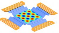 |
| This image shows a simulation of the electric field distribution in a two-dimensional standing surface wave field.
Credit: Tony Jun Huang, Penn State |
Abstract:
The smaller components become, the more difficult it is to create patterns in an economical and reproducible way, according to an interdisciplinary team of Penn State researchers who, using sound waves, can place nanowires in repeatable patterns for potential use in a variety of sensors, optoelectronics and nanoscale circuits.
Sound waves precisely position nanowires
Philadelphia, PA | Posted on June 19th, 2013"There are ways to create these devices with lithography, but it is very hard to create patterns below 50 nanometers using lithography," said Tony Jun Huang, associate professor of engineering science and mechanics, Penn State. "It is rather simple now to make metal nanomaterials using synthetic chemistry. Our process allows pattern transfer of arrays of these nanomaterials onto substrates that might not be compatible with conventional lithography. For example, we could make networks of wires and then pattern them to arrays of living cells."
The researchers looked at the placement of metallic nanowires in solution on a piezoelectric substrate. Piezoelectric materials move when an electric voltage is applied to them and create an electric voltage when compressed.
In this case, the researchers applied an alternating current to the substrate so that the material's movement creates a standing surface acoustic wave in the solution. A standing wave has node locations that do not move, so the nanowires arrive at these nodes and remain there.
If the researchers apply only one current, then the nanowires form a one-dimensional array with the nanowires lined up head to tail in parallel rows. If perpendicular currents are used, a two-dimensional grid of standing waves forms and the nanowires move to those grid-point nodes and form a three-dimensional spark-like pattern.
"Because the pitch of both the one-dimensional and two-dimensional structures is sensitive to the frequency of the standing surface acoustic wave field, this technique allows for the patterning of nanowires with tunable spacing and density," the researchers report in a recent issue of ACS Nano. The nanowires in solution will settle in place onto the substrate when the solution evaporates, preserving the pattern. The researchers note that the patterned nanowires could then be transferred to organic polymer substrates with good accuracy by placing the polymer onto the top of the nanowires and with slight pressure, transferring the nanowires. They suggest that the nanowires could then be transferred to rigid or flexible substrates from the organic polymer using microcontact-printing techniques that are well developed.
"We really think our technique can be extremely powerful," said Huang. "We can tune the pattern to the configuration we want and then transfer the nanowires using a polymer stamp."
The spacing of the nodes where nanowires deposit can be adjusted on the fly by changing the frequency and the interaction between the two electric fields.
"This would save a lot of time compared to lithography or other static fabrication methods," said Huang. The researchers are currently investigating more complex designs.
###
Other researchers working on this project include Yuchao Chen, Xiaoyun Ding, Sz-Chin Steven Lin, Po-Hsun Huang, Nitesh Nama, Yanhui Zhao, Ahmad Ahsan Nawaz and Feng Guo, all graduate students in engineering science and mechanics; Shikuan Yang, postdoctoral researcher in engineering science and mechanics; Yeyi Gu, graduate student in food science; and Thomas E. Mallouk, Evan Pugh Professor of Chemistry, and Wei Wang, graduate student in chemistry.
The National Institutes of Health, National Science Foundation and the Penn State Center for Nanoscale Science supported this research.
####
For more information, please click here
Contacts:
A'ndrea Elyse Messer
814-865-9481
Copyright © Penn State
If you have a comment, please Contact us.Issuers of news releases, not 7th Wave, Inc. or Nanotechnology Now, are solely responsible for the accuracy of the content.
Bookmark:


| Related News Press |
News and information
![]() Quantum computer improves AI predictions April 17th, 2026
Quantum computer improves AI predictions April 17th, 2026
![]() Flexible sensor gains sensitivity under pressure April 17th, 2026
Flexible sensor gains sensitivity under pressure April 17th, 2026
![]() A reusable chip for particulate matter sensing April 17th, 2026
A reusable chip for particulate matter sensing April 17th, 2026
![]() Detecting vibrational quantum beating in the predissociation dynamics of SF6 using time-resolved photoelectron spectroscopy April 17th, 2026
Detecting vibrational quantum beating in the predissociation dynamics of SF6 using time-resolved photoelectron spectroscopy April 17th, 2026
Govt.-Legislation/Regulation/Funding/Policy
![]() Quantum computer improves AI predictions April 17th, 2026
Quantum computer improves AI predictions April 17th, 2026
![]() Metasurfaces smooth light to boost magnetic sensing precision January 30th, 2026
Metasurfaces smooth light to boost magnetic sensing precision January 30th, 2026
![]() New imaging approach transforms study of bacterial biofilms August 8th, 2025
New imaging approach transforms study of bacterial biofilms August 8th, 2025
Chip Technology
![]() A reusable chip for particulate matter sensing April 17th, 2026
A reusable chip for particulate matter sensing April 17th, 2026
![]() Metasurfaces smooth light to boost magnetic sensing precision January 30th, 2026
Metasurfaces smooth light to boost magnetic sensing precision January 30th, 2026
Optical computing/Photonic computing
![]() ICFO researchers overcome long-standing bottleneck in single photon detection with twisted 2D materials August 8th, 2025
ICFO researchers overcome long-standing bottleneck in single photon detection with twisted 2D materials August 8th, 2025
![]() Programmable electron-induced color router array May 14th, 2025
Programmable electron-induced color router array May 14th, 2025
Sensors
![]() Flexible sensor gains sensitivity under pressure April 17th, 2026
Flexible sensor gains sensitivity under pressure April 17th, 2026
![]() Tiny nanosheets, big leap: A new sensor detects ethanol at ultra-low levels January 30th, 2026
Tiny nanosheets, big leap: A new sensor detects ethanol at ultra-low levels January 30th, 2026
![]() From sensors to smart systems: the rise of AI-driven photonic noses January 30th, 2026
From sensors to smart systems: the rise of AI-driven photonic noses January 30th, 2026
![]() Sensors innovations for smart lithium-based batteries: advancements, opportunities, and potential challenges August 8th, 2025
Sensors innovations for smart lithium-based batteries: advancements, opportunities, and potential challenges August 8th, 2025
Nanoelectronics
![]() Lab to industry: InSe wafer-scale breakthrough for future electronics August 8th, 2025
Lab to industry: InSe wafer-scale breakthrough for future electronics August 8th, 2025
![]() Interdisciplinary: Rice team tackles the future of semiconductors Multiferroics could be the key to ultralow-energy computing October 6th, 2023
Interdisciplinary: Rice team tackles the future of semiconductors Multiferroics could be the key to ultralow-energy computing October 6th, 2023
![]() Key element for a scalable quantum computer: Physicists from Forschungszentrum J�lich and RWTH Aachen University demonstrate electron transport on a quantum chip September 23rd, 2022
Key element for a scalable quantum computer: Physicists from Forschungszentrum J�lich and RWTH Aachen University demonstrate electron transport on a quantum chip September 23rd, 2022
![]() Reduced power consumption in semiconductor devices September 23rd, 2022
Reduced power consumption in semiconductor devices September 23rd, 2022
Discoveries
![]() Quantum computer improves AI predictions April 17th, 2026
Quantum computer improves AI predictions April 17th, 2026
![]() Flexible sensor gains sensitivity under pressure April 17th, 2026
Flexible sensor gains sensitivity under pressure April 17th, 2026
![]() A reusable chip for particulate matter sensing April 17th, 2026
A reusable chip for particulate matter sensing April 17th, 2026
![]() Detecting vibrational quantum beating in the predissociation dynamics of SF6 using time-resolved photoelectron spectroscopy April 17th, 2026
Detecting vibrational quantum beating in the predissociation dynamics of SF6 using time-resolved photoelectron spectroscopy April 17th, 2026
Announcements
![]() A fundamentally new therapeutic approach to cystic fibrosis: Nanobody repairs cellular defect April 17th, 2026
A fundamentally new therapeutic approach to cystic fibrosis: Nanobody repairs cellular defect April 17th, 2026
![]() UC Irvine physicists discover method to reverse �quantum scrambling� : The work addresses the problem of information loss in quantum computing system April 17th, 2026
UC Irvine physicists discover method to reverse �quantum scrambling� : The work addresses the problem of information loss in quantum computing system April 17th, 2026
Battery Technology/Capacitors/Generators/Piezoelectrics/Thermoelectrics/Energy storage
![]() Decoding hydrogen‑bond network of electrolyte for cryogenic durable aqueous zinc‑ion batteries January 30th, 2026
Decoding hydrogen‑bond network of electrolyte for cryogenic durable aqueous zinc‑ion batteries January 30th, 2026
![]() COF scaffold membrane with gate‑lane nanostructure for efficient Li+/Mg2+ separation January 30th, 2026
COF scaffold membrane with gate‑lane nanostructure for efficient Li+/Mg2+ separation January 30th, 2026
![]() MXene nanomaterials enter a new dimension Multilayer nanomaterial: MXene flakes created at Drexel University show new promise as 1D scrolls January 30th, 2026
MXene nanomaterials enter a new dimension Multilayer nanomaterial: MXene flakes created at Drexel University show new promise as 1D scrolls January 30th, 2026
Printing/Lithography/Inkjet/Inks/Bio-printing/Dyes
![]() Presenting: Ultrasound-based printing of 3D materials�potentially inside the body December 8th, 2023
Presenting: Ultrasound-based printing of 3D materials�potentially inside the body December 8th, 2023
![]() Simple ballpoint pen can write custom LEDs August 11th, 2023
Simple ballpoint pen can write custom LEDs August 11th, 2023
![]() Disposable electronics on a simple sheet of paper October 7th, 2022
Disposable electronics on a simple sheet of paper October 7th, 2022
|
|
||
|
|
||
| The latest news from around the world, FREE | ||
|
|
||
|
|
||
| Premium Products | ||
|
|
||
|
Only the news you want to read!
Learn More |
||
|
|
||
|
Full-service, expert consulting
Learn More |
||
|
|
||