Home > Press > Nanowires grown on graphene have surprising structure
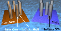 |
| Graphic by
Parsian Mohseni
Schematic representation of phase segregated InGaAs/InAs nanowires grown on graphene and single phase InGaAs nanowires grown on a different substrate |
Abstract:
When a team of University of Illinois engineers set out to grow nanowires of a compound semiconductor on top of a sheet of graphene, they did not expect to discover a new paradigm of epitaxy.
Nanowires grown on graphene have surprising structure
Champaign, IL | Posted on April 22nd, 2013The self-assembled wires have a core of one composition and an outer layer of another, a desired trait for many advanced electronics applications. Led by professor Xiuling Li, in collaboration with professors Eric Pop and Joseph Lyding, all professors of electrical and computer engineering, the team published its findings in the journal Nano Letters.
Nanowires, tiny strings of semiconductor material, have great potential for applications in transistors, solar cells, lasers, sensors and more.
"Nanowires are really the major building blocks of future nano-devices," said postdoctoral researcher Parsian Mohseni, first author of the study. "Nanowires are components that can be used, based on what material you grow them out of, for any functional electronics application."
Li's group uses a method called van der Waals epitaxy to grow nanowires from the bottom up on a flat substrate of semiconductor materials, such as silicon. The nanowires are made of a class of materials called III-V (three-five), compound semiconductors that hold particular promise for applications involving light, such as solar cells or lasers.
The group previously reported growing III-V nanowires on silicon. While silicon is the most widely used material in devices, it has a number of shortcomings. Now, the group has grown nanowires of the material indium gallium arsenide (InGaAs) on a sheet of graphene, a 1-atom-thick sheet of carbon with exceptional physical and conductive properties.
Thanks to its thinness, graphene is flexible, while silicon is rigid and brittle. It also conducts like a metal, allowing for direct electrical contact to the nanowires. Furthermore, it is inexpensive, flaked off from a block of graphite or grown from carbon gases.
"One of the reasons we want to grow on graphene is to stay away from thick and expensive substrates," Mohseni said. "About 80 percent of the manufacturing cost of a conventional solar cell comes from the substrate itself. We've done away with that by just using graphene. Not only are there inherent cost benefits, we're also introducing functionality that a typical substrate doesn't have."
The researchers pump gases containing gallium, indium and arsenic into a chamber with a graphene sheet. The nanowires self-assemble, growing by themselves into a dense carpet of vertical wires across the surface of the graphene. Other groups have grown nanowires on graphene with compound semiconductors that only have two elements, but by using three elements, the Illinois group made a unique finding: The InGaAs wires grown on graphene spontaneously segregate into an indium arsenide (InAs) core with an InGaAs shell around the outside of the wire.
"This is unexpected," Li said. "A lot of devices require a core-shell architecture. Normally you grow the core in one growth condition and change conditions to grow the shell on the outside. This is spontaneous, done in one step. The other good thing is that since it's a spontaneous segregation, it produces a perfect interface."
So what causes this spontaneous core-shell structure? By coincidence, the distance between atoms in a crystal of InAs is nearly the same as the distance between whole numbers of carbon atoms in a sheet of graphene. So, when the gases are piped into the chamber and the material begins to crystallize, InAs settles into place on the graphene, a near-perfect fit, while the gallium compound settles on the outside of the wires. This was unexpected, because normally, with van der Waals epitaxy, the respective crystal structures of the material and the substrate are not supposed to matter.
"We didn't expect it, but once we saw it, it made sense," Mohseni said.
In addition, by tuning the ratio of gallium to indium in the semiconductor cocktail, the researchers can tune the optical and conductive properties of the nanowires.
Next, Li's group plans to make solar cells and other optoelectronic devices with their graphene-grown nanowires. Thanks to both the wires' ternary composition and graphene's flexibility and conductivity, Li hopes to integrate the wires in a broad spectrum of applications.
"We basically discovered a new phenomenon that confirms that registry does count in van der Waals epitaxy," Li said.
This work was supported in part by the Department of Energy and the National Science Foundation. Postdoctoral researcher Ashkan Behnam and graduate students Joshua Wood and Christopher English also were co-authors of the paper. Li also is affiliated with the Beckman Institute for Advanced Science and Technology, the Micro and Nanotechnology Lab, and the Frederick Seitz Materials Research Lab, all at the U. of I.
####
For more information, please click here
Contacts:
Liz Ahlberg
Physical Sciences Editor
217-244-1073
Xiuling Li
217-265-6354
Copyright © University of Illinois at Urbana-Champaign
If you have a comment, please Contact us.Issuers of news releases, not 7th Wave, Inc. or Nanotechnology Now, are solely responsible for the accuracy of the content.
Bookmark:


| Related Links |
| Related News Press |
News and information
![]() Quantum computer improves AI predictions April 17th, 2026
Quantum computer improves AI predictions April 17th, 2026
![]() Flexible sensor gains sensitivity under pressure April 17th, 2026
Flexible sensor gains sensitivity under pressure April 17th, 2026
![]() A reusable chip for particulate matter sensing April 17th, 2026
A reusable chip for particulate matter sensing April 17th, 2026
![]() Detecting vibrational quantum beating in the predissociation dynamics of SF6 using time-resolved photoelectron spectroscopy April 17th, 2026
Detecting vibrational quantum beating in the predissociation dynamics of SF6 using time-resolved photoelectron spectroscopy April 17th, 2026
Graphene/ Graphite
![]() Electrifying results shed light on graphene foam as a potential material for lab grown cartilage June 6th, 2025
Electrifying results shed light on graphene foam as a potential material for lab grown cartilage June 6th, 2025
![]() Breakthrough in proton barrier films using pore-free graphene oxide: Kumamoto University researchers achieve new milestone in advanced coating technologies September 13th, 2024
Breakthrough in proton barrier films using pore-free graphene oxide: Kumamoto University researchers achieve new milestone in advanced coating technologies September 13th, 2024
Govt.-Legislation/Regulation/Funding/Policy
![]() Quantum computer improves AI predictions April 17th, 2026
Quantum computer improves AI predictions April 17th, 2026
![]() Metasurfaces smooth light to boost magnetic sensing precision January 30th, 2026
Metasurfaces smooth light to boost magnetic sensing precision January 30th, 2026
![]() New imaging approach transforms study of bacterial biofilms August 8th, 2025
New imaging approach transforms study of bacterial biofilms August 8th, 2025
Chip Technology
![]() A reusable chip for particulate matter sensing April 17th, 2026
A reusable chip for particulate matter sensing April 17th, 2026
![]() Metasurfaces smooth light to boost magnetic sensing precision January 30th, 2026
Metasurfaces smooth light to boost magnetic sensing precision January 30th, 2026
Self Assembly
![]() Diamond glitter: A play of colors with artificial DNA crystals May 17th, 2024
Diamond glitter: A play of colors with artificial DNA crystals May 17th, 2024
![]() Liquid crystal templated chiral nanomaterials October 14th, 2022
Liquid crystal templated chiral nanomaterials October 14th, 2022
![]() Nanoclusters self-organize into centimeter-scale hierarchical assemblies April 22nd, 2022
Nanoclusters self-organize into centimeter-scale hierarchical assemblies April 22nd, 2022
![]() Atom by atom: building precise smaller nanoparticles with templates March 4th, 2022
Atom by atom: building precise smaller nanoparticles with templates March 4th, 2022
Optical computing/Photonic computing
![]() ICFO researchers overcome long-standing bottleneck in single photon detection with twisted 2D materials August 8th, 2025
ICFO researchers overcome long-standing bottleneck in single photon detection with twisted 2D materials August 8th, 2025
![]() Programmable electron-induced color router array May 14th, 2025
Programmable electron-induced color router array May 14th, 2025
Nanoelectronics
![]() Lab to industry: InSe wafer-scale breakthrough for future electronics August 8th, 2025
Lab to industry: InSe wafer-scale breakthrough for future electronics August 8th, 2025
![]() Interdisciplinary: Rice team tackles the future of semiconductors Multiferroics could be the key to ultralow-energy computing October 6th, 2023
Interdisciplinary: Rice team tackles the future of semiconductors Multiferroics could be the key to ultralow-energy computing October 6th, 2023
![]() Key element for a scalable quantum computer: Physicists from Forschungszentrum J�lich and RWTH Aachen University demonstrate electron transport on a quantum chip September 23rd, 2022
Key element for a scalable quantum computer: Physicists from Forschungszentrum J�lich and RWTH Aachen University demonstrate electron transport on a quantum chip September 23rd, 2022
![]() Reduced power consumption in semiconductor devices September 23rd, 2022
Reduced power consumption in semiconductor devices September 23rd, 2022
Discoveries
![]() Quantum computer improves AI predictions April 17th, 2026
Quantum computer improves AI predictions April 17th, 2026
![]() Flexible sensor gains sensitivity under pressure April 17th, 2026
Flexible sensor gains sensitivity under pressure April 17th, 2026
![]() A reusable chip for particulate matter sensing April 17th, 2026
A reusable chip for particulate matter sensing April 17th, 2026
![]() Detecting vibrational quantum beating in the predissociation dynamics of SF6 using time-resolved photoelectron spectroscopy April 17th, 2026
Detecting vibrational quantum beating in the predissociation dynamics of SF6 using time-resolved photoelectron spectroscopy April 17th, 2026
Announcements
![]() A fundamentally new therapeutic approach to cystic fibrosis: Nanobody repairs cellular defect April 17th, 2026
A fundamentally new therapeutic approach to cystic fibrosis: Nanobody repairs cellular defect April 17th, 2026
![]() UC Irvine physicists discover method to reverse �quantum scrambling� : The work addresses the problem of information loss in quantum computing system April 17th, 2026
UC Irvine physicists discover method to reverse �quantum scrambling� : The work addresses the problem of information loss in quantum computing system April 17th, 2026
Energy
![]() Sensors innovations for smart lithium-based batteries: advancements, opportunities, and potential challenges August 8th, 2025
Sensors innovations for smart lithium-based batteries: advancements, opportunities, and potential challenges August 8th, 2025
![]() Simple algorithm paired with standard imaging tool could predict failure in lithium metal batteries August 8th, 2025
Simple algorithm paired with standard imaging tool could predict failure in lithium metal batteries August 8th, 2025
Photonics/Optics/Lasers
![]() Metasurfaces smooth light to boost magnetic sensing precision January 30th, 2026
Metasurfaces smooth light to boost magnetic sensing precision January 30th, 2026
![]() From sensors to smart systems: the rise of AI-driven photonic noses January 30th, 2026
From sensors to smart systems: the rise of AI-driven photonic noses January 30th, 2026
Solar/Photovoltaic
![]() Spinel-type sulfide semiconductors to operate the next-generation LEDs and solar cells For solar-cell absorbers and green-LED source October 3rd, 2025
Spinel-type sulfide semiconductors to operate the next-generation LEDs and solar cells For solar-cell absorbers and green-LED source October 3rd, 2025
![]() KAIST researchers introduce new and improved, next-generation perovskite solar cell November 8th, 2024
KAIST researchers introduce new and improved, next-generation perovskite solar cell November 8th, 2024
![]() Groundbreaking precision in single-molecule optoelectronics August 16th, 2024
Groundbreaking precision in single-molecule optoelectronics August 16th, 2024
![]() Development of zinc oxide nanopagoda array photoelectrode: photoelectrochemical water-splitting hydrogen production January 12th, 2024
Development of zinc oxide nanopagoda array photoelectrode: photoelectrochemical water-splitting hydrogen production January 12th, 2024
|
|
||
|
|
||
| The latest news from around the world, FREE | ||
|
|
||
|
|
||
| Premium Products | ||
|
|
||
|
Only the news you want to read!
Learn More |
||
|
|
||
|
Full-service, expert consulting
Learn More |
||
|
|
||