Home > Press > NRL Researchers Discover New Route to Spin-Polarized Contacts on Silicon
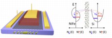 |
| NRL scientists successfully used graphene, a single layer of carbon atoms in a honeycomb lattice (gray), as a tunnel barrier to electrically inject spin polarized electrons from a ferromagnetic NiFe contact (red) into a silicon substrate (purple). The net spin accumulation in the silicon produces a voltage, which can be directly measured. Spin injection, manipulation and detection are the fundamental elements allowing information processing with the electron spin rather than its charge. (Image: U.S. Naval Research Laboratory) |
Abstract:
Scientists at the Naval Research Laboratory have demonstrated that graphene, a single layer of carbon atoms in a honeycomb lattice, can serve as a low resistance spin-polarized tunnel barrier contact which successfully enables spin injection/detection in silicon from a ferromagnetic metal. The graphene provides a highly uniform, chemically inert and thermally robust tunnel barrier free of defects and trap states which plague oxide barriers. This discovery clears an important hurdle to the development of future semiconductor spintronic devices, that is, devices which rely on manipulating the electron's spin rather than its charge for low-power, high-speed information processing beyond the traditional size scaling of Moore's Law. The research results are reported in a paper published in Nature Nanotechnology on September 30, 2012 (DOI 10.1038/nnano.2012.161).
NRL Researchers Discover New Route to Spin-Polarized Contacts on Silicon
Washington, DC | Posted on October 23rd, 2012Ferromagnetic metals, such as iron or permalloy, have intrinsically spin-polarized electron populations (more "spin-up" electrons than "spin-down", see figure), and are thus ideal contacts for injection and detection of spin in a semiconductor. An intervening tunnel barrier is required to avoid saturation of both semiconductor spin channels by the much larger metal conductivity - this would otherwise result in no net spin polarization in the semiconductor. However, the oxide barriers typically used (such as Al2O3 or MgO) introduce defects, trapped charge and interdiffusion, and have resistances, which are too high - all of these factors severely impact the performance. To solve this problem, the NRL research team, led by Dr. Berend Jonker, used single layer graphene as the tunnel barrier. This novel approach utilizes a defect resistant, chemically inert and stable material with well-controlled thickness to achieve a low resistance spin contact compatible with both the ferromagnetic metal and semiconductor of choice. These qualities insure minimal diffusion to/ and from the surrounding materials at temperatures required for device manufacturing.
The research team used this approach to demonstrate electrical generation and detection of spin accumulation in silicon above room temperature, and showed that the contact resistance-area products are 100 to 1000 times lower than achieved with oxide tunnel barriers on silicon substrates with identical doping levels.
These results identify a new route to low resistance-area product spin-polarized contacts, a key requirement for semiconductor spintronic devices that rely upon two-terminal magnetoresistance, including spin-based transistors, logic and memory, explains NRL's Dr. Berend Jonker.
In looking to the future, the NRL team suggests that the use of multilayer graphene in such structures may provide much higher values of the tunnel spin polarization due to band structure derived spin filtering effects which have been predicted for selected ferromagnetic metal / multi-layer graphene structures. This increase would improve the performance of semiconductor spintronic devices by providing higher signal to noise ratios and corresponding operating speeds, advancing the techological applications of silicon spintronics.
The NRL research team includes Dr. Olaf van 't Erve, Dr. Adam Friedman, Dr. Enrique Cobas, Dr. Connie Li, and Dr. Berend Jonker from the Materials Science and Technology Division, and Dr. Jeremy Robinson from the Electronics Science and Technology Division.
####
About Naval Research Laboratory
The U.S. Naval Research Laboratory is the Navy's full-spectrum corporate laboratory, conducting a broadly based multidisciplinary program of scientific research and advanced technological development. The Laboratory, with a total complement of nearly 2,500 personnel, is located in southwest Washington, D.C., with other major sites at the Stennis Space Center, Miss., and Monterey, Calif. NRL has served the Navy and the nation for over 85 years and continues to meet the complex technological challenges of today's world. For more information, visit the NRL homepage or join the conversation on Twitter, Facebook, and YouTube.
For more information, please click here
Contacts:
Donna McKinney
(202) 767-2541
Copyright © U.S. Naval Research Laboratory
If you have a comment, please Contact us.Issuers of news releases, not 7th Wave, Inc. or Nanotechnology Now, are solely responsible for the accuracy of the content.
Bookmark:


| Related News Press |
News and information
![]() Quantum computer improves AI predictions April 17th, 2026
Quantum computer improves AI predictions April 17th, 2026
![]() Flexible sensor gains sensitivity under pressure April 17th, 2026
Flexible sensor gains sensitivity under pressure April 17th, 2026
![]() A reusable chip for particulate matter sensing April 17th, 2026
A reusable chip for particulate matter sensing April 17th, 2026
![]() Detecting vibrational quantum beating in the predissociation dynamics of SF6 using time-resolved photoelectron spectroscopy April 17th, 2026
Detecting vibrational quantum beating in the predissociation dynamics of SF6 using time-resolved photoelectron spectroscopy April 17th, 2026
Graphene/ Graphite
![]() Electrifying results shed light on graphene foam as a potential material for lab grown cartilage June 6th, 2025
Electrifying results shed light on graphene foam as a potential material for lab grown cartilage June 6th, 2025
![]() Breakthrough in proton barrier films using pore-free graphene oxide: Kumamoto University researchers achieve new milestone in advanced coating technologies September 13th, 2024
Breakthrough in proton barrier films using pore-free graphene oxide: Kumamoto University researchers achieve new milestone in advanced coating technologies September 13th, 2024
Govt.-Legislation/Regulation/Funding/Policy
![]() Quantum computer improves AI predictions April 17th, 2026
Quantum computer improves AI predictions April 17th, 2026
![]() Metasurfaces smooth light to boost magnetic sensing precision January 30th, 2026
Metasurfaces smooth light to boost magnetic sensing precision January 30th, 2026
![]() New imaging approach transforms study of bacterial biofilms August 8th, 2025
New imaging approach transforms study of bacterial biofilms August 8th, 2025
Spintronics
![]() Quantum materials: Electron spin measured for the first time June 9th, 2023
Quantum materials: Electron spin measured for the first time June 9th, 2023
Chip Technology
![]() A reusable chip for particulate matter sensing April 17th, 2026
A reusable chip for particulate matter sensing April 17th, 2026
![]() Metasurfaces smooth light to boost magnetic sensing precision January 30th, 2026
Metasurfaces smooth light to boost magnetic sensing precision January 30th, 2026
Discoveries
![]() Quantum computer improves AI predictions April 17th, 2026
Quantum computer improves AI predictions April 17th, 2026
![]() Flexible sensor gains sensitivity under pressure April 17th, 2026
Flexible sensor gains sensitivity under pressure April 17th, 2026
![]() A reusable chip for particulate matter sensing April 17th, 2026
A reusable chip for particulate matter sensing April 17th, 2026
![]() Detecting vibrational quantum beating in the predissociation dynamics of SF6 using time-resolved photoelectron spectroscopy April 17th, 2026
Detecting vibrational quantum beating in the predissociation dynamics of SF6 using time-resolved photoelectron spectroscopy April 17th, 2026
Announcements
![]() A fundamentally new therapeutic approach to cystic fibrosis: Nanobody repairs cellular defect April 17th, 2026
A fundamentally new therapeutic approach to cystic fibrosis: Nanobody repairs cellular defect April 17th, 2026
![]() UC Irvine physicists discover method to reverse �quantum scrambling� : The work addresses the problem of information loss in quantum computing system April 17th, 2026
UC Irvine physicists discover method to reverse �quantum scrambling� : The work addresses the problem of information loss in quantum computing system April 17th, 2026
Military
![]() Quantum engineers �squeeze� laser frequency combs to make more sensitive gas sensors January 17th, 2025
Quantum engineers �squeeze� laser frequency combs to make more sensitive gas sensors January 17th, 2025
![]() Chainmail-like material could be the future of armor: First 2D mechanically interlocked polymer exhibits exceptional flexibility and strength January 17th, 2025
Chainmail-like material could be the future of armor: First 2D mechanically interlocked polymer exhibits exceptional flexibility and strength January 17th, 2025
![]() Single atoms show their true color July 5th, 2024
Single atoms show their true color July 5th, 2024
![]() NRL charters Navy�s quantum inertial navigation path to reduce drift April 5th, 2024
NRL charters Navy�s quantum inertial navigation path to reduce drift April 5th, 2024
|
|
||
|
|
||
| The latest news from around the world, FREE | ||
|
|
||
|
|
||
| Premium Products | ||
|
|
||
|
Only the news you want to read!
Learn More |
||
|
|
||
|
Full-service, expert consulting
Learn More |
||
|
|
||