Home > Press > FEI Launches New Helios NanoLab HP Platform for High Productivity TEM Sample Preparation: New DualBeam systems enable expedited process development, helping chipmakers improve yield ramp by making vital process improvement decisions faster
 |
Abstract:
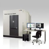
FEI (NASDAQ: FEIC), a leading instrumentation company providing imaging and analysis systems for research and industry, today announced new Helios NanoLab™ DualBeam™ systems for engineers that need to make vital process improvement decisions. The 450HP and 1200HP DualBeam systems include new capability that meets the critical requirements for semiconductor process development at the 28nm device geometry node and below.
FEI Launches New Helios NanoLab HP Platform for High Productivity TEM Sample Preparation: New DualBeam systems enable expedited process development, helping chipmakers improve yield ramp by making vital process improvement decisions faster
Hillsboro, OR | Posted on August 28th, 2012"Developing new processes and technologies that include shrinking geometries, new materials and novel device architectures and ramping those processes to high-volume production quickly are driving unprecedented increases in the demand for TEM analysis," stated Rudy Kellner, vice president and general manager, Electronics Business Unit, FEI. "TEM samples must be ultra-thin, of the highest quality, and generated in a routine and consistent manner across a fleet of tools. Typically, as samples get thinner, the difficulty becomes time to results, operator skill level and subtle differences among equipment. We have designed the 450HP and 1200HP systems to overcome these issues. Ultimately, the system's ability to yield more good samples at double the throughput allows for potentially significant reductions for both the time-to-answer and the cost-per-answer."
The Helios NanoLab 450HP and 1200HP DualBeam systems can prepare 15nm thick samples with less than a 2nm damage layer in 90 minutes, two times faster than competitive alternatives. iFast™ automation software maximizes ease-of-use while ensuring consistency among multiple operators and systems. QuickFlip grid holders facilitate inverted sample preparation to improve sample quality while maintaining high throughput. Cell Navigation software allows automated navigation within non-unique memory arrays that can locate a single designated bit cell in a 50nm lateral field. Together, these features enable a robust process to prepare high quality, ultra-thin lamella across multiple tools in a consistent manner—independent of operator skill level.
The Helios NanoLab 450HP and 1200HP DualBeam systems are available for ordering immediately. The 450HP model can accommodate samples up to 100mm, while the 1200HP system can handle full 300mm wafers. For more information, please visit: www.FEI.com/TemPrep .
####
About FEI Company
FEI (Nasdaq: FEIC) is a leading diversified scientific instruments company. It is a premier provider of electron- and ion-beam microscopes and solutions for nanoscale applications across many industries: industrial and academic materials research, life sciences, semiconductors, data storage, natural resources and more. With more than 60 years of technological innovation and leadership, FEI has set the performance standard in transmission electron microscopes (TEM), scanning electron microscopes (SEM) and DualBeams™, which combine a SEM with a focused ion beam (FIB). Headquartered in Hillsboro, Ore., USA, FEI has over 2,300 employees and sales and service operations in more than 50 countries around the world. More information can be found at: www.fei.com.
FEI Safe Harbor Statement
This news release contains forward-looking statements that include statements regarding the performance capabilities and benefits of the Helios NanoLab 450HP and 1200HP DualBeam systems. Factors that could affect these forward-looking statements include but are not limited to failure of the product or technology to perform as expected and achieve anticipated results, unexpected technology problems and challenges, changes to the technology, the inability of FEI, its suppliers or project partners to make the technological advances required for the technology to achieve anticipated results, the inability of customers to develop and deploy the expected new applications and our ability to manufacture, ship and deliver the tools or software as expected. Please also refer to our Form 10-K, Forms 10-Q, Forms 8-K and other filings with the U.S. Securities and Exchange Commission for additional information on these factors and other factors that could cause actual results to differ materially from the forward-looking statements. FEI assumes no duty to update forward-looking statements.
For more information, please click here
Contacts:
Sandy Fewkes
Principal
(media contact)
MindWrite Communications, Inc
+1 408 224 4024
FEI Company
Fletcher Chamberlin
(investors and analysts)
Investor Relations
+1 503 726 7710
Copyright © FEI Company
If you have a comment, please Contact us.Issuers of news releases, not 7th Wave, Inc. or Nanotechnology Now, are solely responsible for the accuracy of the content.
Bookmark:


| Related News Press |
News and information
![]() Quantum computer improves AI predictions April 17th, 2026
Quantum computer improves AI predictions April 17th, 2026
![]() Flexible sensor gains sensitivity under pressure April 17th, 2026
Flexible sensor gains sensitivity under pressure April 17th, 2026
![]() A reusable chip for particulate matter sensing April 17th, 2026
A reusable chip for particulate matter sensing April 17th, 2026
![]() Detecting vibrational quantum beating in the predissociation dynamics of SF6 using time-resolved photoelectron spectroscopy April 17th, 2026
Detecting vibrational quantum beating in the predissociation dynamics of SF6 using time-resolved photoelectron spectroscopy April 17th, 2026
Imaging
![]() Simple algorithm paired with standard imaging tool could predict failure in lithium metal batteries August 8th, 2025
Simple algorithm paired with standard imaging tool could predict failure in lithium metal batteries August 8th, 2025
Chip Technology
![]() A reusable chip for particulate matter sensing April 17th, 2026
A reusable chip for particulate matter sensing April 17th, 2026
![]() Metasurfaces smooth light to boost magnetic sensing precision January 30th, 2026
Metasurfaces smooth light to boost magnetic sensing precision January 30th, 2026
Announcements
![]() A fundamentally new therapeutic approach to cystic fibrosis: Nanobody repairs cellular defect April 17th, 2026
A fundamentally new therapeutic approach to cystic fibrosis: Nanobody repairs cellular defect April 17th, 2026
![]() UC Irvine physicists discover method to reverse ‘quantum scrambling’ : The work addresses the problem of information loss in quantum computing system April 17th, 2026
UC Irvine physicists discover method to reverse ‘quantum scrambling’ : The work addresses the problem of information loss in quantum computing system April 17th, 2026
Tools
![]() Metasurfaces smooth light to boost magnetic sensing precision January 30th, 2026
Metasurfaces smooth light to boost magnetic sensing precision January 30th, 2026
![]() From sensors to smart systems: the rise of AI-driven photonic noses January 30th, 2026
From sensors to smart systems: the rise of AI-driven photonic noses January 30th, 2026
![]() Japan launches fully domestically produced quantum computer: Expo visitors to experience quantum computing firsthand August 8th, 2025
Japan launches fully domestically produced quantum computer: Expo visitors to experience quantum computing firsthand August 8th, 2025
|
|
||
|
|
||
| The latest news from around the world, FREE | ||
|
|
||
|
|
||
| Premium Products | ||
|
|
||
|
Only the news you want to read!
Learn More |
||
|
|
||
|
Full-service, expert consulting
Learn More |
||
|
|
||