Home > Press > Taming light with graphene: Scientists visualize the trapping and confinement of light on graphene, making a sheet of carbon atoms the most promising candidate for optical information processing on the nano-scale, optical detection, and ultrafast optoelectronics
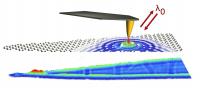 |
| This image shows optical nanoimaging of graphene plasmons. The upper panel shows a sketch of the imaging method. A laser illuminated scanning tip launches plasmons on graphene. Detection is by recording the light backscattered from the tip. The lower panel shows optical image of graphene, where the fringes visualize the interference of the graphene plasmons.
Credit: nanoGUNE, IQFR-CSIC, ICFO |
Abstract:
Spanish research groups achieve first ever visualizations of light guided with nanometric precision on graphene (a one-atom-thick sheet of carbon atoms). This visualization proves what theoretical physicists have long predicted; that it is possible to trap and manipulate light in a highly efficient way, using graphene as a novel platform for optical information processing and sensing. Synergies between theoretical proposals from IQFR-CSIC (Madrid), specializations in graphene nano-photonics and nano-optoelectonics at ICFO (Barcelona), and experimental expertise in optical nano-imaging at nanoGUNE (San Sebastian) give rise to these noteworthy results reported in Nature this week in a back-to-back publication alongside a similar study by the group of Dmitry Basov in UCSD in California.
Taming light with graphene: Scientists visualize the trapping and confinement of light on graphene, making a sheet of carbon atoms the most promising candidate for optical information processing on the nano-scale, optical detection, and ultrafast optoelectronics
Spain | Posted on June 20th, 2012Graphene is a material that, among many other fascinating properties, has an extraordinary optical behavior. Particularly interesting optical properties had been predicted for the case that light couples to so-called plasmons, wave-like excitations that were predicted to exist in the "sea" of conduction electrons of graphene. However, no direct experimental evidence of plasmons in graphene had been shown up to this work. This is because the wavelength of graphene plasmons is 10 to 100 times smaller than what can be seen with conventional light microscopes. Now, the researchers show the first experimental images of graphene plasmons. They used a so called near-field microscope that uses a sharp tip to convert the illumination light into a nanoscale light spot that provides the extra push needed for the plasmons to be created. At the same time the tip probes the presence of plasmons (see figure). Rainer Hillenbrand, leader of the nanoGUNE group comments: "Seeing is believing! Our near-field optical images definitely proof the existence of propagating and localized graphene plasmons and allow for a direct measurement of their dramatically reduced wavelength."
As demonstrated by the researchers, graphene plasmons can be used to electrically control light in a similar fashion as is traditionally achieved with electrons in a transistor. These capabilities, which until now were impossible with other existing plasmonic materials, enable new highly efficient nano-scale optical switches which can perform calculations using light instead of electricity. "With our work we show that graphene is an excellent choice for solving the long-standing and technologically important problem of modulating light at the speeds of today's microchips," says Javier Garc�a de Abajo, leader of the IQFR-CSIC group. In addition, the capability of trapping light in very small volumes could give rise to a new generation of nano-sensors with applications in diverse areas such as medicine and bio-detection, solar cells and light detectors, as well as quantum information processing. This result literally opens a new field of research and provides a first viable path towards ultrafast tuning of light, which was not possible until now. Frank Koppens, leader of the ICFO group, summarizes: "Graphene is a novel and unique material for plasmonics, truly bridging the fields of nano-electronics and nano-optics".
###
Published manuscript:
Optical nano-imaging of gate-tunable graphene plasmons Jianing Chen, Michela Badioli, Pablo Alonso-Gonz�lez, Susokin Thongrattanasiri, Florian Huth, Johann Osmond, Marko Spasenović, Alba Centeno, Amaia Pesquera, Philippe Godignon, Amaia Zurutuza, Nicolas Camara, Javier Garc�a de Abajo, Rainer Hillenbrand & Frank Koppens
DOI: 10.1038/nature11254
Contributions and institutes:
Optical nano-imaging: CIC nanoGUNE Consolider (San Sebastian, Spain), CFM-CSIC-UPV/EHU (San Sebastian, Spain), Neaspec GmbH (Martinsried, Germany), Ikerbasque (Bilbao, Spain)
Graphene nano-photonics and optoelectronics: ICFO (Barcelona, Spain)
Theory: IQFR-CSIC (Madrid, Spain)
Graphene synthesis: Graphenea (San Sebastian, Spain) University of Tours (Tours, France), and CNM-IMB-CSIC (Barcelona, Spain)
####
For more information, please click here
Contacts:
Aitziber Lasa Iglesias
34-943-363-040
Copyright © Elhuyar Fundazioa
If you have a comment, please Contact us.Issuers of news releases, not 7th Wave, Inc. or Nanotechnology Now, are solely responsible for the accuracy of the content.
Bookmark:


| Related News Press |
News and information
![]() Quantum computer improves AI predictions April 17th, 2026
Quantum computer improves AI predictions April 17th, 2026
![]() Flexible sensor gains sensitivity under pressure April 17th, 2026
Flexible sensor gains sensitivity under pressure April 17th, 2026
![]() A reusable chip for particulate matter sensing April 17th, 2026
A reusable chip for particulate matter sensing April 17th, 2026
![]() Detecting vibrational quantum beating in the predissociation dynamics of SF6 using time-resolved photoelectron spectroscopy April 17th, 2026
Detecting vibrational quantum beating in the predissociation dynamics of SF6 using time-resolved photoelectron spectroscopy April 17th, 2026
Imaging
![]() Simple algorithm paired with standard imaging tool could predict failure in lithium metal batteries August 8th, 2025
Simple algorithm paired with standard imaging tool could predict failure in lithium metal batteries August 8th, 2025
Graphene/ Graphite
![]() Electrifying results shed light on graphene foam as a potential material for lab grown cartilage June 6th, 2025
Electrifying results shed light on graphene foam as a potential material for lab grown cartilage June 6th, 2025
![]() Breakthrough in proton barrier films using pore-free graphene oxide: Kumamoto University researchers achieve new milestone in advanced coating technologies September 13th, 2024
Breakthrough in proton barrier films using pore-free graphene oxide: Kumamoto University researchers achieve new milestone in advanced coating technologies September 13th, 2024
Chip Technology
![]() A reusable chip for particulate matter sensing April 17th, 2026
A reusable chip for particulate matter sensing April 17th, 2026
![]() Metasurfaces smooth light to boost magnetic sensing precision January 30th, 2026
Metasurfaces smooth light to boost magnetic sensing precision January 30th, 2026
Quantum Computing
![]() Quantum computer improves AI predictions April 17th, 2026
Quantum computer improves AI predictions April 17th, 2026
![]() UC Irvine physicists discover method to reverse �quantum scrambling� : The work addresses the problem of information loss in quantum computing system April 17th, 2026
UC Irvine physicists discover method to reverse �quantum scrambling� : The work addresses the problem of information loss in quantum computing system April 17th, 2026
![]() Researchers develop molecular qubits that communicate at telecom frequencies October 3rd, 2025
Researchers develop molecular qubits that communicate at telecom frequencies October 3rd, 2025
Optical computing/Photonic computing
![]() ICFO researchers overcome long-standing bottleneck in single photon detection with twisted 2D materials August 8th, 2025
ICFO researchers overcome long-standing bottleneck in single photon detection with twisted 2D materials August 8th, 2025
![]() Programmable electron-induced color router array May 14th, 2025
Programmable electron-induced color router array May 14th, 2025
Sensors
![]() Flexible sensor gains sensitivity under pressure April 17th, 2026
Flexible sensor gains sensitivity under pressure April 17th, 2026
![]() Tiny nanosheets, big leap: A new sensor detects ethanol at ultra-low levels January 30th, 2026
Tiny nanosheets, big leap: A new sensor detects ethanol at ultra-low levels January 30th, 2026
![]() From sensors to smart systems: the rise of AI-driven photonic noses January 30th, 2026
From sensors to smart systems: the rise of AI-driven photonic noses January 30th, 2026
![]() Sensors innovations for smart lithium-based batteries: advancements, opportunities, and potential challenges August 8th, 2025
Sensors innovations for smart lithium-based batteries: advancements, opportunities, and potential challenges August 8th, 2025
Discoveries
![]() Quantum computer improves AI predictions April 17th, 2026
Quantum computer improves AI predictions April 17th, 2026
![]() Flexible sensor gains sensitivity under pressure April 17th, 2026
Flexible sensor gains sensitivity under pressure April 17th, 2026
![]() A reusable chip for particulate matter sensing April 17th, 2026
A reusable chip for particulate matter sensing April 17th, 2026
![]() Detecting vibrational quantum beating in the predissociation dynamics of SF6 using time-resolved photoelectron spectroscopy April 17th, 2026
Detecting vibrational quantum beating in the predissociation dynamics of SF6 using time-resolved photoelectron spectroscopy April 17th, 2026
Announcements
![]() A fundamentally new therapeutic approach to cystic fibrosis: Nanobody repairs cellular defect April 17th, 2026
A fundamentally new therapeutic approach to cystic fibrosis: Nanobody repairs cellular defect April 17th, 2026
![]() UC Irvine physicists discover method to reverse �quantum scrambling� : The work addresses the problem of information loss in quantum computing system April 17th, 2026
UC Irvine physicists discover method to reverse �quantum scrambling� : The work addresses the problem of information loss in quantum computing system April 17th, 2026
Tools
![]() Metasurfaces smooth light to boost magnetic sensing precision January 30th, 2026
Metasurfaces smooth light to boost magnetic sensing precision January 30th, 2026
![]() From sensors to smart systems: the rise of AI-driven photonic noses January 30th, 2026
From sensors to smart systems: the rise of AI-driven photonic noses January 30th, 2026
![]() Japan launches fully domestically produced quantum computer: Expo visitors to experience quantum computing firsthand August 8th, 2025
Japan launches fully domestically produced quantum computer: Expo visitors to experience quantum computing firsthand August 8th, 2025
Photonics/Optics/Lasers
![]() Metasurfaces smooth light to boost magnetic sensing precision January 30th, 2026
Metasurfaces smooth light to boost magnetic sensing precision January 30th, 2026
![]() From sensors to smart systems: the rise of AI-driven photonic noses January 30th, 2026
From sensors to smart systems: the rise of AI-driven photonic noses January 30th, 2026
Research partnerships
![]() Lab to industry: InSe wafer-scale breakthrough for future electronics August 8th, 2025
Lab to industry: InSe wafer-scale breakthrough for future electronics August 8th, 2025
![]() HKU physicists uncover hidden order in the quantum world through deconfined quantum critical points April 25th, 2025
HKU physicists uncover hidden order in the quantum world through deconfined quantum critical points April 25th, 2025
Solar/Photovoltaic
![]() Spinel-type sulfide semiconductors to operate the next-generation LEDs and solar cells For solar-cell absorbers and green-LED source October 3rd, 2025
Spinel-type sulfide semiconductors to operate the next-generation LEDs and solar cells For solar-cell absorbers and green-LED source October 3rd, 2025
![]() KAIST researchers introduce new and improved, next-generation perovskite solar cell November 8th, 2024
KAIST researchers introduce new and improved, next-generation perovskite solar cell November 8th, 2024
![]() Groundbreaking precision in single-molecule optoelectronics August 16th, 2024
Groundbreaking precision in single-molecule optoelectronics August 16th, 2024
![]() Development of zinc oxide nanopagoda array photoelectrode: photoelectrochemical water-splitting hydrogen production January 12th, 2024
Development of zinc oxide nanopagoda array photoelectrode: photoelectrochemical water-splitting hydrogen production January 12th, 2024
|
|
||
|
|
||
| The latest news from around the world, FREE | ||
|
|
||
|
|
||
| Premium Products | ||
|
|
||
|
Only the news you want to read!
Learn More |
||
|
|
||
|
Full-service, expert consulting
Learn More |
||
|
|
||