Home > Press > Picosun introduces several industrially scalable ALD processes Source: Picosun Oy
 |
Abstract:
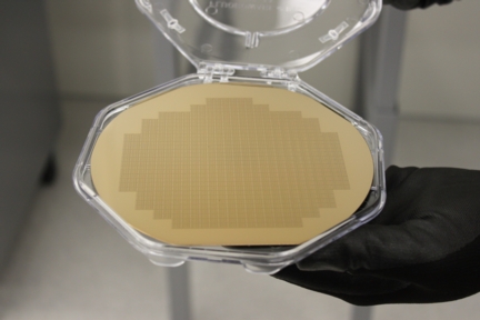
Picosun Oy, Finland-based global manufacturer of state-of-the-art Atomic Layer Deposition (ALD) equipment, has successfully scaled up several new, important ALD processes. Of compound materials, various new sulfides, e.g. Gd2O2S (based on the process originally developed by Prof. Mikko Ritala's group at University of Helsinki, Finland), indium sulfide and zinc sulfide, and oxides, e.g. antimony oxide and Al2O3/Ta2O5 nanolaminates and mixed oxides (also at lower temperatures), are now available for industrial scale processes. Of metals, gold, copper, silver and ruthenium, and of metallic compound materials, TiAlCN and TiN, have also been successfully deposited by novel ALD processes on industrial scale wafer sizes.
Picosun introduces several industrially scalable ALD processes Source: Picosun Oy
Espoo, Finland | Posted on November 30th, 2011The new sulfides and oxides have various applications in e.g. optics, electronics and display industries and as multifunctional protective layers. ALD deposited metal/metallic layers, on the other hand, find their customers especially in MEMS/NEMS (Micro/Nanoelectromechanical systems) and other electronics and integrated circuits industries, where e.g. through-silicon-vias (TSV) and other high aspect ratio (HAR) structures are a common approach in modern 3D-stacked chip architectures. When the via or HAR trench dimensions narrow down to nanometer scale, ALD is the only possible thin film coating method with which e.g. contact metallization, seed, barrier or adhesion layers can be deposited with satisfactory conformality, uniformity and pinhole-free quality.
"In order to keep our spearheading position in serving world-class industrial customers, it is of utmost importance to stay in the lead also in ALD process development. Picosun's close connections to top level ALD research groups worldwide and the unrivaled ALD expertise of our own personnel make Picosun always your number one partner, not only as ALD equipment provider, but also in ALD process development. With Picosun's efficient and innovative production-scale high throughput ALD tool design, the process scale-up is fast and easy and never compromises Picosun's trademark, unparalleledly excellent film and process quality," summarizes Picosun's Managing Director Juhana Kostamo.
####
About Picosun Oy
Picosun Oy is a Finland-based global manufacturer of state-of-the-art ALD systems, representing continuity to almost four decades of dedicated, exclusive ALD reactor design and manufacturing. Picosun�s global headquarters are located in Espoo, Finland, its production facilities in Masala, Kirkkonummi, and its US headquarters in Detroit, Michigan. Picosun�s SUNALE� ALD tools are chosen for production by various industries across four continents. Picosun Oy is a part of Stephen Industries Inc. Oy.
For more information, please click here
Contacts:
Mr. Juhana Kostamo
Phone: +358 50 321 1955
Fax: +358 20 722 7012
Copyright © Picosun Oy
If you have a comment, please Contact us.Issuers of news releases, not 7th Wave, Inc. or Nanotechnology Now, are solely responsible for the accuracy of the content.
| Related News Press |
News and information
![]() Quantum computer improves AI predictions April 17th, 2026
Quantum computer improves AI predictions April 17th, 2026
![]() Flexible sensor gains sensitivity under pressure April 17th, 2026
Flexible sensor gains sensitivity under pressure April 17th, 2026
![]() A reusable chip for particulate matter sensing April 17th, 2026
A reusable chip for particulate matter sensing April 17th, 2026
![]() Detecting vibrational quantum beating in the predissociation dynamics of SF6 using time-resolved photoelectron spectroscopy April 17th, 2026
Detecting vibrational quantum beating in the predissociation dynamics of SF6 using time-resolved photoelectron spectroscopy April 17th, 2026
Chip Technology
![]() A reusable chip for particulate matter sensing April 17th, 2026
A reusable chip for particulate matter sensing April 17th, 2026
![]() Metasurfaces smooth light to boost magnetic sensing precision January 30th, 2026
Metasurfaces smooth light to boost magnetic sensing precision January 30th, 2026
Announcements
![]() A fundamentally new therapeutic approach to cystic fibrosis: Nanobody repairs cellular defect April 17th, 2026
A fundamentally new therapeutic approach to cystic fibrosis: Nanobody repairs cellular defect April 17th, 2026
![]() UC Irvine physicists discover method to reverse �quantum scrambling� : The work addresses the problem of information loss in quantum computing system April 17th, 2026
UC Irvine physicists discover method to reverse �quantum scrambling� : The work addresses the problem of information loss in quantum computing system April 17th, 2026
Tools
![]() Metasurfaces smooth light to boost magnetic sensing precision January 30th, 2026
Metasurfaces smooth light to boost magnetic sensing precision January 30th, 2026
![]() From sensors to smart systems: the rise of AI-driven photonic noses January 30th, 2026
From sensors to smart systems: the rise of AI-driven photonic noses January 30th, 2026
![]() Japan launches fully domestically produced quantum computer: Expo visitors to experience quantum computing firsthand August 8th, 2025
Japan launches fully domestically produced quantum computer: Expo visitors to experience quantum computing firsthand August 8th, 2025
Industrial
![]() Tiny nanosheets, big leap: A new sensor detects ethanol at ultra-low levels January 30th, 2026
Tiny nanosheets, big leap: A new sensor detects ethanol at ultra-low levels January 30th, 2026
![]() Quantum interference in molecule-surface collisions February 28th, 2025
Quantum interference in molecule-surface collisions February 28th, 2025
![]() Boron nitride nanotube fibers get real: Rice lab creates first heat-tolerant, stable fibers from wet-spinning process June 24th, 2022
Boron nitride nanotube fibers get real: Rice lab creates first heat-tolerant, stable fibers from wet-spinning process June 24th, 2022
|
|
||
|
|
||
| The latest news from around the world, FREE | ||
|
|
||
|
|
||
| Premium Products | ||
|
|
||
|
Only the news you want to read!
Learn More |
||
|
|
||
|
Full-service, expert consulting
Learn More |
||
|
|
||


