Home > Press > Periodic structures in organic light-emitters can efficiently enhance and replenish surface plasmon waves
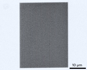 |
| A scanning electron microscope image of an organic grating used to excite surface plasmons |
Abstract:
The irradiation of a metal surface with light or electrons can result in the formation of coherent electronic oscillations called surface plasmons, an effect ideal for applications such as optical communications on optoelectronic chips. Unfortunately, however, surface plasmons quickly lose their energy during transit, limiting their on-chip propagation distance. Jing Hua Teng at the A*STAR Institute of Materials Research and Engineering and co-workers from Nankai University and Nanyang Technological University under the Singapore-China Joint Research Program have now developed nanoscale structures that are able to replenish as well as guide surface plasmons on chips[1]. "These structures can be used as plasmonic sources for lab-on-a-chip applications," says Teng.
Periodic structures in organic light-emitters can efficiently enhance and replenish surface plasmon waves
Singapore | Posted on June 9th, 2011At the resonance frequency, surface plasmons can generate intense light fields close to the surface, especially in metallic nanostructures. For this reason, surface plasmons have been widely studied for a variety of sensing and light-focusing applications. However, the electrical resistance of metals inevitably causes losses in the movements of the electronic currents involved in surface plasmons. It is therefore important to develop schemes that are able to regenerate surface plasmons as they travel along the surface of a chip.
One possibility is the use of organic light-emitting molecules such as rhodamine B. The researchers embedded molecules of rhodamine B in a polymer matrix that was then poured onto the surface of a silver film. To couple the light emission from rhodamine B to the surface plasmons, the polymer layer was structured into a periodic grating (pictured) matched to the resonance frequency of the plasmons. Adjusting the shape and periodicity of the grating allows the light emitted from the surface plasmons to be tailored.
Similar gratings are also used as mirrors in conventional on-chip semiconductor lasers. This structural similarity raises the possibility of combining the plasmonic effects demonstrated here with existing laser designs�an approach that could well lead to the realization of a plasmonic laser.
The advantage of a plasmonic laser over a semiconductor laser is that it can be made much smaller, which is important for the miniaturization of photonic circuits and on-chip sensing applications. "However, such lasers are difficult to fabricate," says Teng. "A number of challenges remain, including how to sufficiently confine the surface plasmons between the mirrors in this kind of configuration and how to reduce the metal damping losses."
Whether for applications in sensing or the on-chip manipulation of light, the potential of these gratings for replenishing plasmons represents an important step toward making plasmonics the key technology for photonic applications in nanoscience.
The A*STAR-affiliated researchers contributing to this research are from the Institute of Materials Research and Engineering
Journal information
[1] Zhang, D. G., Yuan, X. C. & Teng, J. H. Surface plasmon-coupled emission on metallic film coated with dye-doped polymer nanogratings. Applied Physics Letters 97, 231117 (2010).
####
For more information, please click here
Contacts:
Lee Swee Heng
Copyright © The Agency for Science, Technology and Research (A*STAR)
If you have a comment, please Contact us.Issuers of news releases, not 7th Wave, Inc. or Nanotechnology Now, are solely responsible for the accuracy of the content.
Bookmark:


| Related Links |
| Related News Press |
News and information
![]() Quantum computer improves AI predictions April 17th, 2026
Quantum computer improves AI predictions April 17th, 2026
![]() Flexible sensor gains sensitivity under pressure April 17th, 2026
Flexible sensor gains sensitivity under pressure April 17th, 2026
![]() A reusable chip for particulate matter sensing April 17th, 2026
A reusable chip for particulate matter sensing April 17th, 2026
![]() Detecting vibrational quantum beating in the predissociation dynamics of SF6 using time-resolved photoelectron spectroscopy April 17th, 2026
Detecting vibrational quantum beating in the predissociation dynamics of SF6 using time-resolved photoelectron spectroscopy April 17th, 2026
Display technology/LEDs/SS Lighting/OLEDs
![]() Spinel-type sulfide semiconductors to operate the next-generation LEDs and solar cells For solar-cell absorbers and green-LED source October 3rd, 2025
Spinel-type sulfide semiconductors to operate the next-generation LEDs and solar cells For solar-cell absorbers and green-LED source October 3rd, 2025
![]() Efficient and stable hybrid perovskite-organic light-emitting diodes with external quantum efficiency exceeding 40 per cent July 5th, 2024
Efficient and stable hybrid perovskite-organic light-emitting diodes with external quantum efficiency exceeding 40 per cent July 5th, 2024
Lab-on-a-chip
![]() Micro-scale opto-thermo-mechanical actuation in the dry adhesive regime Peer-Reviewed Publication September 24th, 2021
Micro-scale opto-thermo-mechanical actuation in the dry adhesive regime Peer-Reviewed Publication September 24th, 2021
![]() Silicon-graphene hybrid plasmonic waveguide photodetectors beyond 1.55 μm March 13th, 2020
Silicon-graphene hybrid plasmonic waveguide photodetectors beyond 1.55 μm March 13th, 2020
Sensors
![]() Flexible sensor gains sensitivity under pressure April 17th, 2026
Flexible sensor gains sensitivity under pressure April 17th, 2026
![]() Tiny nanosheets, big leap: A new sensor detects ethanol at ultra-low levels January 30th, 2026
Tiny nanosheets, big leap: A new sensor detects ethanol at ultra-low levels January 30th, 2026
![]() From sensors to smart systems: the rise of AI-driven photonic noses January 30th, 2026
From sensors to smart systems: the rise of AI-driven photonic noses January 30th, 2026
![]() Sensors innovations for smart lithium-based batteries: advancements, opportunities, and potential challenges August 8th, 2025
Sensors innovations for smart lithium-based batteries: advancements, opportunities, and potential challenges August 8th, 2025
Discoveries
![]() Quantum computer improves AI predictions April 17th, 2026
Quantum computer improves AI predictions April 17th, 2026
![]() Flexible sensor gains sensitivity under pressure April 17th, 2026
Flexible sensor gains sensitivity under pressure April 17th, 2026
![]() A reusable chip for particulate matter sensing April 17th, 2026
A reusable chip for particulate matter sensing April 17th, 2026
![]() Detecting vibrational quantum beating in the predissociation dynamics of SF6 using time-resolved photoelectron spectroscopy April 17th, 2026
Detecting vibrational quantum beating in the predissociation dynamics of SF6 using time-resolved photoelectron spectroscopy April 17th, 2026
Announcements
![]() A fundamentally new therapeutic approach to cystic fibrosis: Nanobody repairs cellular defect April 17th, 2026
A fundamentally new therapeutic approach to cystic fibrosis: Nanobody repairs cellular defect April 17th, 2026
![]() UC Irvine physicists discover method to reverse �quantum scrambling� : The work addresses the problem of information loss in quantum computing system April 17th, 2026
UC Irvine physicists discover method to reverse �quantum scrambling� : The work addresses the problem of information loss in quantum computing system April 17th, 2026
Photonics/Optics/Lasers
![]() Metasurfaces smooth light to boost magnetic sensing precision January 30th, 2026
Metasurfaces smooth light to boost magnetic sensing precision January 30th, 2026
![]() From sensors to smart systems: the rise of AI-driven photonic noses January 30th, 2026
From sensors to smart systems: the rise of AI-driven photonic noses January 30th, 2026
|
|
||
|
|
||
| The latest news from around the world, FREE | ||
|
|
||
|
|
||
| Premium Products | ||
|
|
||
|
Only the news you want to read!
Learn More |
||
|
|
||
|
Full-service, expert consulting
Learn More |
||
|
|
||