Home > Press > New Stanford Nano Center provides state-of-the-art equipment for research at the smallest of scales: Stanford has significantly upgraded its nanotechnology research with a new Nano Center, providing faculty with some of the world's best nanoscale research facilities
 |
|
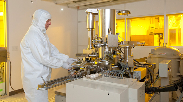
Photo by L.A. Cicero Senior research scientist Rich Tiberio prepares to use the JEOL 6300 ebeam lithography system. |
Abstract:
BY SANDEEP RAVINDRAN
Stanford researchers now have access to the latest and greatest tools to explore the strange and promising world of nanomaterials. The new labs and equipment could pave the way for better solar cells, more efficient batteries and new tools to detect and treat cancers.
New Stanford Nano Center provides state-of-the-art equipment for research at the smallest of scales: Stanford has significantly upgraded its nanotechnology research with a new Nano Center, providing faculty with some of the world's best nanoscale research facilities
Stanford, CA | Posted on March 23rd, 2011The Stanford Nano Center, along with the existing Nanofabrication Facility and Nanocharacterization Laboratory, will upgrade the university's nanotechnology facilities to rank among the best in the world.
The staff of the Nano Center's shared facilities has begun training and working with students and researchers; instruments will continue to become operational throughout the spring and summer.
A nanometer is a billionth of a meter, about the size of a few atoms. "It's a very exciting length," said Kathryn Moler, associate professor of physics and applied physics who has been coordinating the development of the new center since 2007. At those scales, "physics, biology and chemistry all intersect," she said.
"Nanoscale research has the potential to advance every field of technology," Moler said. In energy research, nanotechnology could help scientists design more efficient platinum catalysts for fuel cells. In medicine, nanoparticles can be used for targeted drug delivery and for enhanced medical imaging. And nanotechnology is expected to advance the state of electronics.
Apart from the practical applications, the new tools will also help researchers answer fundamental questions about quantum mechanics and the nature of matter.
"Things have different properties at that scale," said Moler. "For example, a one-meter piece of gold is gold-colored. But as pieces of gold get smaller than 100 nanometers, they have many different colors and optical properties."
A 2006 survey of Stanford faculty members revealed 77 labs across campus that were interested in using the latest nanotechnology equipment. But the equipment is large and expensive, and must often be protected from the smallest of vibrations from the outside world. "Scientists need different tools to see and manipulate things that are a billionth of a meter," Moler said. "It's a whole new frontier.
"We decided instead of building these facilities in 77 different labs, we could build one lab with shared tools."
The Stanford Nano Center is housed in the engineering quad, with 2,400 square feet on the first floor and 6,000 square feet under the main plaza. Building the structure underground reduces vibrations and keeps temperatures stable. The power supply and other utilities are housed off-site to minimize electromagnetic interference.
The center also contains several clean rooms that are kept free of dust, which could otherwise contaminate nanomaterials. And unlike many traditional clean rooms that can only be used to work on silicon, the first floor of the Nano Center has "flexible" clean rooms where researchers can work on any element they need for their research.
These clean rooms are "a thousand times cleaner than your normal office," said Richard Tiberio, a Nano Center staff member. He believes the facility has "turned a corner with the new year. We're done tightening bolts, and now we're ready to build things." The facility can routinely build objects as small as a hundred nanometers, and can build handcrafted items as small as ten nanometers, Tiberio said.
Like some of the Nano Center's other expert staff, Tiberio splits time among the university's three nanomaterials facilities. Roger Howe is the faculty director of one of these facilities, the Stanford Nanofabrication Facility. "There's a long history of nanotechnology at Stanford," he said.
"The neatest things about the new center are the wonderful instruments in it," Howe said. They make "things that were at the edge of possibility become routine."
Howe said the new equipment, such as the "amazing" new electron microscopes, will accelerate student research. "For my students, it's like a new candy store just opened up," he said. "We'd love to sample all the new things we can do with these new tools".
Anyone walking through the corridors will be able to see all these sophisticated tools in use. "There's a tendency to put this kind of equipment in dark closets," said Ann Arvin, Stanford's Dean of Research. "We built the equipment rooms with a glass wall so people can see in."
Arvin believes the Nano Center will help attract students and new faculty to the university. "Facilities like this enable new research, that's what's really important," she said. "If every instrument costs $6 million to $10 million, no one investigator can equip his lab with all this equipment.
"I expect this will help faculty and students be competitive despite tight research funding. To do cutting-edge experiments they require cutting-edge equipment," she said.
The new facilities will be used by faculty from many different fields. This was why the university, its president, several other deans and departments, and individual faculty all came together to make it a reality, Arvin said.
Moler and electrical engineering Professor H.-S. Philip Wong headed a faculty committee to decide what equipment the new facility should have. Highlights include a microscope that can measure extremely small magnetic fields. "It's unique for a research facility," said Moler.
In addition, a couple of electron microscopes will let researchers get a detailed look at nanomaterials, and they can also use an electron beam to print tiny patterns on wafers for use in electronics. Scientists will also have access to one of the most sensitive mass spectrometers in the world, which will allow them to analyze even minute quantities of materials.
"I'm excited to use the new facility," said Robert Sinclair, director of the Stanford Nanocharacterization Laboratory. "The university had great vision. Ten years ago we were behind other leading universities, but now our capabilities have leap-frogged others to rank among the best."
Sandeep Ravindran is a science-writing intern at the Stanford News Service.
####
For more information, please click here
Contacts:
Stanford, CA 94305
(650) 723-2300
Dan Stober
Stanford News Service:
(650) 721-6965
Copyright © Stanford University
If you have a comment, please Contact us.Issuers of news releases, not 7th Wave, Inc. or Nanotechnology Now, are solely responsible for the accuracy of the content.
Bookmark:


| Related Links |
![]() Stanford Nanocharacterization Facility
Stanford Nanocharacterization Facility
![]() Stanford Nanofabrication Facility
Stanford Nanofabrication Facility
| Related News Press |
News and information
![]() Quantum computer improves AI predictions April 17th, 2026
Quantum computer improves AI predictions April 17th, 2026
![]() Flexible sensor gains sensitivity under pressure April 17th, 2026
Flexible sensor gains sensitivity under pressure April 17th, 2026
![]() A reusable chip for particulate matter sensing April 17th, 2026
A reusable chip for particulate matter sensing April 17th, 2026
![]() Detecting vibrational quantum beating in the predissociation dynamics of SF6 using time-resolved photoelectron spectroscopy April 17th, 2026
Detecting vibrational quantum beating in the predissociation dynamics of SF6 using time-resolved photoelectron spectroscopy April 17th, 2026
Imaging
![]() Simple algorithm paired with standard imaging tool could predict failure in lithium metal batteries August 8th, 2025
Simple algorithm paired with standard imaging tool could predict failure in lithium metal batteries August 8th, 2025
Possible Futures
![]() A fundamentally new therapeutic approach to cystic fibrosis: Nanobody repairs cellular defect April 17th, 2026
A fundamentally new therapeutic approach to cystic fibrosis: Nanobody repairs cellular defect April 17th, 2026
![]() UC Irvine physicists discover method to reverse �quantum scrambling� : The work addresses the problem of information loss in quantum computing system April 17th, 2026
UC Irvine physicists discover method to reverse �quantum scrambling� : The work addresses the problem of information loss in quantum computing system April 17th, 2026
Academic/Education
![]() Rice University launches Rice Synthetic Biology Institute to improve lives January 12th, 2024
Rice University launches Rice Synthetic Biology Institute to improve lives January 12th, 2024
![]() Multi-institution, $4.6 million NSF grant to fund nanotechnology training September 9th, 2022
Multi-institution, $4.6 million NSF grant to fund nanotechnology training September 9th, 2022
Nanomedicine
![]() A fundamentally new therapeutic approach to cystic fibrosis: Nanobody repairs cellular defect April 17th, 2026
A fundamentally new therapeutic approach to cystic fibrosis: Nanobody repairs cellular defect April 17th, 2026
![]() New molecular technology targets tumors and simultaneously silences two �undruggable� cancer genes August 8th, 2025
New molecular technology targets tumors and simultaneously silences two �undruggable� cancer genes August 8th, 2025
![]() New imaging approach transforms study of bacterial biofilms August 8th, 2025
New imaging approach transforms study of bacterial biofilms August 8th, 2025
![]() Electrifying results shed light on graphene foam as a potential material for lab grown cartilage June 6th, 2025
Electrifying results shed light on graphene foam as a potential material for lab grown cartilage June 6th, 2025
Announcements
![]() A fundamentally new therapeutic approach to cystic fibrosis: Nanobody repairs cellular defect April 17th, 2026
A fundamentally new therapeutic approach to cystic fibrosis: Nanobody repairs cellular defect April 17th, 2026
![]() UC Irvine physicists discover method to reverse �quantum scrambling� : The work addresses the problem of information loss in quantum computing system April 17th, 2026
UC Irvine physicists discover method to reverse �quantum scrambling� : The work addresses the problem of information loss in quantum computing system April 17th, 2026
Tools
![]() Metasurfaces smooth light to boost magnetic sensing precision January 30th, 2026
Metasurfaces smooth light to boost magnetic sensing precision January 30th, 2026
![]() From sensors to smart systems: the rise of AI-driven photonic noses January 30th, 2026
From sensors to smart systems: the rise of AI-driven photonic noses January 30th, 2026
![]() Japan launches fully domestically produced quantum computer: Expo visitors to experience quantum computing firsthand August 8th, 2025
Japan launches fully domestically produced quantum computer: Expo visitors to experience quantum computing firsthand August 8th, 2025
Energy
![]() Sensors innovations for smart lithium-based batteries: advancements, opportunities, and potential challenges August 8th, 2025
Sensors innovations for smart lithium-based batteries: advancements, opportunities, and potential challenges August 8th, 2025
![]() Simple algorithm paired with standard imaging tool could predict failure in lithium metal batteries August 8th, 2025
Simple algorithm paired with standard imaging tool could predict failure in lithium metal batteries August 8th, 2025
Battery Technology/Capacitors/Generators/Piezoelectrics/Thermoelectrics/Energy storage
![]() Decoding hydrogen‑bond network of electrolyte for cryogenic durable aqueous zinc‑ion batteries January 30th, 2026
Decoding hydrogen‑bond network of electrolyte for cryogenic durable aqueous zinc‑ion batteries January 30th, 2026
![]() COF scaffold membrane with gate‑lane nanostructure for efficient Li+/Mg2+ separation January 30th, 2026
COF scaffold membrane with gate‑lane nanostructure for efficient Li+/Mg2+ separation January 30th, 2026
![]() MXene nanomaterials enter a new dimension Multilayer nanomaterial: MXene flakes created at Drexel University show new promise as 1D scrolls January 30th, 2026
MXene nanomaterials enter a new dimension Multilayer nanomaterial: MXene flakes created at Drexel University show new promise as 1D scrolls January 30th, 2026
Solar/Photovoltaic
![]() Spinel-type sulfide semiconductors to operate the next-generation LEDs and solar cells For solar-cell absorbers and green-LED source October 3rd, 2025
Spinel-type sulfide semiconductors to operate the next-generation LEDs and solar cells For solar-cell absorbers and green-LED source October 3rd, 2025
![]() KAIST researchers introduce new and improved, next-generation perovskite solar cell November 8th, 2024
KAIST researchers introduce new and improved, next-generation perovskite solar cell November 8th, 2024
![]() Groundbreaking precision in single-molecule optoelectronics August 16th, 2024
Groundbreaking precision in single-molecule optoelectronics August 16th, 2024
![]() Development of zinc oxide nanopagoda array photoelectrode: photoelectrochemical water-splitting hydrogen production January 12th, 2024
Development of zinc oxide nanopagoda array photoelectrode: photoelectrochemical water-splitting hydrogen production January 12th, 2024
|
|
||
|
|
||
| The latest news from around the world, FREE | ||
|
|
||
|
|
||
| Premium Products | ||
|
|
||
|
Only the news you want to read!
Learn More |
||
|
|
||
|
Full-service, expert consulting
Learn More |
||
|
|
||