Home > Press > CAMECA Unveils News Semiconductor Metrology Tool
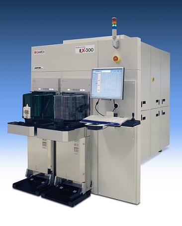 |
| Cameca EX-300 LEXES metrology tool |
Abstract:
Versatile Metrology Tool for Front-End Process Control Of 22nm Technology Nodes and Beyond
CAMECA Unveils News Semiconductor Metrology Tool
Gennevillers, France | Posted on January 27th, 2011CAMECA, a world leader in scientific instrumentation and metrology solutions for semiconductor labs and fabs, has unveiled the latest addition to its line of high-end metrology systems-the EX-300 metrology tool targeted for front-end process control of 22 nm technology nodes and beyond.
"CAMECA is very proud to introduce the EX-300," notes Dr. Michel Schuhmacher, CAMECA Vice President and Chief Technical Officer. "This highly versatile metrology tool benefits from CAMECA's 10-years of experience with LEXES (Low-energy Electron induced X-ray Emission Spectrometry) technology."
"We are convinced that the EX-300 will become the metrology tool of choice for semiconductor fabs integrating new challenging processes," adds Dr. Schuhmacher. "The EX-300 offers unique capabilities for front-end compositional control at and near the surface. The instrument targets front-end process control for 22nm technology nodes and performs metrology of patterned wafers down to 30x30�m."
The EX-300 utilizes LEXES, a unique surface probing technique pioneered by CAMECA. The technology is now well-established for addressing challenges in elemental composition, thickness determination and dopant dosimetry. With dozens of CAMECA LEXFAB 300 instruments currently installed at the top-ten semiconductor fabrication facilities worldwide, the technology is considered the standard for semiconductor R&D and ramping-up phases at the most advanced nodes as well as for high-volume production monitoring.
CAMECA optimized the performance of the EX-300 for challenging High K Metal Gate (HKMG), epitaxial layers such as Boron in Silcon Germanium(B:SiGe) and shallow implants, fulfilling requirements of both rapid device development and high-yield mass production. In addition, the instrument is designed to deliver enhanced long-term stability and minimize mean time to repair (MTTR).
####
About CAMECA
CAMECA has more than 50 years of experience in the design, manufacture and servicing of scientific instruments for material micro- and nano-analysis. Since pioneering Secondary Ion Mass Spectrometry (SIMS) and Electron Probe Microanalysis (EPMA) instrumentation in the 1950s, CAMECA has remained an undisputed world leader, while achieving numerous breakthrough innovations in such complementary techniques as LEXES and Atom Probe Tomography.
More recently CAMECA has evolved successfully from a provider of scientific instrumentation for the international research community to a provider of metrology solutions for the semiconductor industry. Headquartered near Paris, CAMECA has subsidiaries in China, Germany, Japan, Korea, Taiwan and the United States along with a global network of agents. Acquired in 2007 by AMETEK, Inc, a leading global manufacturer of electronic instrument and electromechanical products, CAMECA is now a unit of AMETEK�s Materials Analysis Division.
For more information, please click here
Contacts:
Marion Chopin
+33 (1) 43 34 62 00
Copyright © CAMECA
If you have a comment, please Contact us.Issuers of news releases, not 7th Wave, Inc. or Nanotechnology Now, are solely responsible for the accuracy of the content.
Bookmark:


| Related News Press |
News and information
![]() Quantum computer improves AI predictions April 17th, 2026
Quantum computer improves AI predictions April 17th, 2026
![]() Flexible sensor gains sensitivity under pressure April 17th, 2026
Flexible sensor gains sensitivity under pressure April 17th, 2026
![]() A reusable chip for particulate matter sensing April 17th, 2026
A reusable chip for particulate matter sensing April 17th, 2026
![]() Detecting vibrational quantum beating in the predissociation dynamics of SF6 using time-resolved photoelectron spectroscopy April 17th, 2026
Detecting vibrational quantum beating in the predissociation dynamics of SF6 using time-resolved photoelectron spectroscopy April 17th, 2026
Chip Technology
![]() A reusable chip for particulate matter sensing April 17th, 2026
A reusable chip for particulate matter sensing April 17th, 2026
![]() Metasurfaces smooth light to boost magnetic sensing precision January 30th, 2026
Metasurfaces smooth light to boost magnetic sensing precision January 30th, 2026
Memory Technology
![]() Researchers tackle the memory bottleneck stalling quantum computing October 3rd, 2025
Researchers tackle the memory bottleneck stalling quantum computing October 3rd, 2025
![]() First real-time observation of two-dimensional melting process: Researchers at Mainz University unveil new insights into magnetic vortex structures August 8th, 2025
First real-time observation of two-dimensional melting process: Researchers at Mainz University unveil new insights into magnetic vortex structures August 8th, 2025
![]() Utilizing palladium for addressing contact issues of buried oxide thin film transistors April 5th, 2024
Utilizing palladium for addressing contact issues of buried oxide thin film transistors April 5th, 2024
Nanoelectronics
![]() Lab to industry: InSe wafer-scale breakthrough for future electronics August 8th, 2025
Lab to industry: InSe wafer-scale breakthrough for future electronics August 8th, 2025
![]() Interdisciplinary: Rice team tackles the future of semiconductors Multiferroics could be the key to ultralow-energy computing October 6th, 2023
Interdisciplinary: Rice team tackles the future of semiconductors Multiferroics could be the key to ultralow-energy computing October 6th, 2023
![]() Key element for a scalable quantum computer: Physicists from Forschungszentrum J�lich and RWTH Aachen University demonstrate electron transport on a quantum chip September 23rd, 2022
Key element for a scalable quantum computer: Physicists from Forschungszentrum J�lich and RWTH Aachen University demonstrate electron transport on a quantum chip September 23rd, 2022
![]() Reduced power consumption in semiconductor devices September 23rd, 2022
Reduced power consumption in semiconductor devices September 23rd, 2022
Announcements
![]() A fundamentally new therapeutic approach to cystic fibrosis: Nanobody repairs cellular defect April 17th, 2026
A fundamentally new therapeutic approach to cystic fibrosis: Nanobody repairs cellular defect April 17th, 2026
![]() UC Irvine physicists discover method to reverse �quantum scrambling� : The work addresses the problem of information loss in quantum computing system April 17th, 2026
UC Irvine physicists discover method to reverse �quantum scrambling� : The work addresses the problem of information loss in quantum computing system April 17th, 2026
Tools
![]() Metasurfaces smooth light to boost magnetic sensing precision January 30th, 2026
Metasurfaces smooth light to boost magnetic sensing precision January 30th, 2026
![]() From sensors to smart systems: the rise of AI-driven photonic noses January 30th, 2026
From sensors to smart systems: the rise of AI-driven photonic noses January 30th, 2026
![]() Japan launches fully domestically produced quantum computer: Expo visitors to experience quantum computing firsthand August 8th, 2025
Japan launches fully domestically produced quantum computer: Expo visitors to experience quantum computing firsthand August 8th, 2025
|
|
||
|
|
||
| The latest news from around the world, FREE | ||
|
|
||
|
|
||
| Premium Products | ||
|
|
||
|
Only the news you want to read!
Learn More |
||
|
|
||
|
Full-service, expert consulting
Learn More |
||
|
|
||