Home > Press > How soccer ball molecules push their way under surfaces
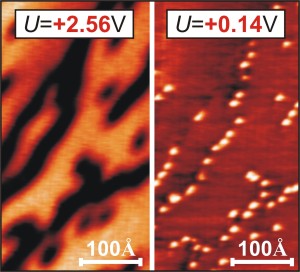 |
| Microscopical image of a graphene layer on a nickel substrate. The image to the left, which was measured at an arbitrary bias voltage of the microscope tip, shows just dark stripes. Only after the bias voltage has spectroscopically been tuned to the very C60 molecules (right), they become visible beneath the graphene layer as the cause of the stripe pattern. |
Abstract:
HZB researchers observe atomic processes while doping semiconductor materials
How soccer ball molecules push their way under surfaces
Berlin | Posted on July 13th, 2010Fullerene and graphene, two forms of carbon only recently discovered, have been stimulating the imaginations of researchers ever since their discovery (fullerene in 1970, graphene in 2004). With graphene especially, researchers see a chance for a new chapter in electronics, since this semiconductor material could one day replace the long-standing key element silicon. For this to happen, it would have to be possible to dope graphene - which is a single-atom layer of graphite - with foreign atoms. And in such a way that the important structural properties of graphene remain intact. In the online preprint of August issue of the journal Advanced Materials (DOI: 10.1002/adma. 201000695) researchers from Helmholtz-Zentrum Berlin f�r Materialien und Energie (HZB) report on a new technique of microscopy. With it, they can show how individual fullerene molecules used for doping push their way under a graphene layer that has been previously deposited onto a nickel substrate.
Graphene is the first crystal known to be stable in two dimensions, because its carbon atoms arrange themselves into a honeycomb structure of hexagons. Fullerene has the addition of pentagons, allowing a spherical structure for which the 60-carbon-atom molecule has made its name as the soccer ball molecule.
Andrei Varykhalov and colleagues deposited a thin layer of graphene onto a nickel substrate using chemical vapour deposition starting with propylene. Next, they inserted individual fullerene molecules between the nickel surface and the graphene layer. They achieved this by rapidly heating the sample to 400 degrees Celsius, followed by brief annealing. The crucial technique that allowed them to observe the fullerene molecules as they squeezed their way in - a process called intercalation - was scanning tunnelling microscopy.
An electrically conductive stylus tip is systematically scanned over the sample surface, which is also conductive. Yet, the tip and object surface never come into contact, so no current flows at first. When the microscope tip comes to within a few tenths of a nanometre of the sample surface, however, the tunnel-ling effect kicks in. That means an exchange of electrons from the sample sur-face and tip starts to take place. If a voltage is then applied, a tunnel current flows, which responds with utmost sensitivity to the tiniest changes in distance.
The HZB researchers set up their scanning tunnelling microscopy experiment such that a clear contrast shows up as soon as the tip of the microscope per-ceives the fullerene molecules beneath the graphene surface. To obtain crucial parameters for this, they first studied the sample using synchrotron radiation at the storage ring BESSY II.
"Using our imaging technique, we can visualize intercalation compounds quite universally," Andrei Varykhalov emphasizes the importance of the experiments. In the development of new semiconductor technology, such an imaging tech-nique is indispensable for developing new components.
####
About Helmholtz-Zentrum Berlin
The Helmholtz-Zentrum Berlin f�r Materialien und Energie (HZB) operates and develops large scale facilities for research with photons (synchrotron beams) and neutrons. The experimental facilities, some of which are unique, are used annually by more than 2,500 guest researchers from universities and other research organisations worldwide. Above all, HZB is known for the unique sam-ple environments that can be created (high magnetic fields, low temperatures). HZB conducts materials research on themes that espe-cially benefit from and are suited to large scale facilities. Research topics include magnetic materials and functional materials.
In the research focus area of solar energy, the development of thin film solar cells is a priority, whilst chemical fuels from sunlight are also a vital research theme. HZB has approx.1,100 employees of whom some 800 work on the Lise-Meitner Campus in Wannsee and 300 on the Wilhelm-Conrad-R�ntgen Campus in Adlershof.
HZB is a member of the Helmholtz Association of German Research Centres, the largest scientific organisation in Germany.
For more information, please click here
Contacts:
Dr. Andrei Varykhalov
(030) 8062-14888
Priv.-Doz. Dr. Oliver Rader
(030) 8062-12950
Press Office
Dr. Ina Helms
(030) 8062-42034
Copyright © Helmholtz-Zentrum Berlin
If you have a comment, please Contact us.Issuers of news releases, not 7th Wave, Inc. or Nanotechnology Now, are solely responsible for the accuracy of the content.
Bookmark:


| Related News Press |
News and information
![]() Quantum computer improves AI predictions April 17th, 2026
Quantum computer improves AI predictions April 17th, 2026
![]() Flexible sensor gains sensitivity under pressure April 17th, 2026
Flexible sensor gains sensitivity under pressure April 17th, 2026
![]() A reusable chip for particulate matter sensing April 17th, 2026
A reusable chip for particulate matter sensing April 17th, 2026
![]() Detecting vibrational quantum beating in the predissociation dynamics of SF6 using time-resolved photoelectron spectroscopy April 17th, 2026
Detecting vibrational quantum beating in the predissociation dynamics of SF6 using time-resolved photoelectron spectroscopy April 17th, 2026
Chemistry
![]() Projecting light to dispense liquids: A new route to ultra-precise microdroplets January 30th, 2026
Projecting light to dispense liquids: A new route to ultra-precise microdroplets January 30th, 2026
![]() From sensors to smart systems: the rise of AI-driven photonic noses January 30th, 2026
From sensors to smart systems: the rise of AI-driven photonic noses January 30th, 2026
![]() "Nanoreactor" cage uses visible light for catalytic and ultra-selective cross-cycloadditions October 3rd, 2025
"Nanoreactor" cage uses visible light for catalytic and ultra-selective cross-cycloadditions October 3rd, 2025
![]() Cambridge chemists discover simple way to build bigger molecules � one carbon at a time June 6th, 2025
Cambridge chemists discover simple way to build bigger molecules � one carbon at a time June 6th, 2025
Thin films
![]() Tiny nanosheets, big leap: A new sensor detects ethanol at ultra-low levels January 30th, 2026
Tiny nanosheets, big leap: A new sensor detects ethanol at ultra-low levels January 30th, 2026
Possible Futures
![]() A fundamentally new therapeutic approach to cystic fibrosis: Nanobody repairs cellular defect April 17th, 2026
A fundamentally new therapeutic approach to cystic fibrosis: Nanobody repairs cellular defect April 17th, 2026
![]() UC Irvine physicists discover method to reverse �quantum scrambling� : The work addresses the problem of information loss in quantum computing system April 17th, 2026
UC Irvine physicists discover method to reverse �quantum scrambling� : The work addresses the problem of information loss in quantum computing system April 17th, 2026
Academic/Education
![]() Rice University launches Rice Synthetic Biology Institute to improve lives January 12th, 2024
Rice University launches Rice Synthetic Biology Institute to improve lives January 12th, 2024
![]() Multi-institution, $4.6 million NSF grant to fund nanotechnology training September 9th, 2022
Multi-institution, $4.6 million NSF grant to fund nanotechnology training September 9th, 2022
Chip Technology
![]() A reusable chip for particulate matter sensing April 17th, 2026
A reusable chip for particulate matter sensing April 17th, 2026
![]() Metasurfaces smooth light to boost magnetic sensing precision January 30th, 2026
Metasurfaces smooth light to boost magnetic sensing precision January 30th, 2026
Nanotubes/Buckyballs/Fullerenes/Nanorods/Nanostrings/Nanosheets
![]() Tiny nanosheets, big leap: A new sensor detects ethanol at ultra-low levels January 30th, 2026
Tiny nanosheets, big leap: A new sensor detects ethanol at ultra-low levels January 30th, 2026
![]() Enhancing power factor of p- and n-type single-walled carbon nanotubes April 25th, 2025
Enhancing power factor of p- and n-type single-walled carbon nanotubes April 25th, 2025
![]() Chainmail-like material could be the future of armor: First 2D mechanically interlocked polymer exhibits exceptional flexibility and strength January 17th, 2025
Chainmail-like material could be the future of armor: First 2D mechanically interlocked polymer exhibits exceptional flexibility and strength January 17th, 2025
![]() Innovative biomimetic superhydrophobic coating combines repair and buffering properties for superior anti-erosion December 13th, 2024
Innovative biomimetic superhydrophobic coating combines repair and buffering properties for superior anti-erosion December 13th, 2024
Nanoelectronics
![]() Lab to industry: InSe wafer-scale breakthrough for future electronics August 8th, 2025
Lab to industry: InSe wafer-scale breakthrough for future electronics August 8th, 2025
![]() Interdisciplinary: Rice team tackles the future of semiconductors Multiferroics could be the key to ultralow-energy computing October 6th, 2023
Interdisciplinary: Rice team tackles the future of semiconductors Multiferroics could be the key to ultralow-energy computing October 6th, 2023
![]() Key element for a scalable quantum computer: Physicists from Forschungszentrum J�lich and RWTH Aachen University demonstrate electron transport on a quantum chip September 23rd, 2022
Key element for a scalable quantum computer: Physicists from Forschungszentrum J�lich and RWTH Aachen University demonstrate electron transport on a quantum chip September 23rd, 2022
![]() Reduced power consumption in semiconductor devices September 23rd, 2022
Reduced power consumption in semiconductor devices September 23rd, 2022
Announcements
![]() A fundamentally new therapeutic approach to cystic fibrosis: Nanobody repairs cellular defect April 17th, 2026
A fundamentally new therapeutic approach to cystic fibrosis: Nanobody repairs cellular defect April 17th, 2026
![]() UC Irvine physicists discover method to reverse �quantum scrambling� : The work addresses the problem of information loss in quantum computing system April 17th, 2026
UC Irvine physicists discover method to reverse �quantum scrambling� : The work addresses the problem of information loss in quantum computing system April 17th, 2026
Tools
![]() Metasurfaces smooth light to boost magnetic sensing precision January 30th, 2026
Metasurfaces smooth light to boost magnetic sensing precision January 30th, 2026
![]() From sensors to smart systems: the rise of AI-driven photonic noses January 30th, 2026
From sensors to smart systems: the rise of AI-driven photonic noses January 30th, 2026
![]() Japan launches fully domestically produced quantum computer: Expo visitors to experience quantum computing firsthand August 8th, 2025
Japan launches fully domestically produced quantum computer: Expo visitors to experience quantum computing firsthand August 8th, 2025
|
|
||
|
|
||
| The latest news from around the world, FREE | ||
|
|
||
|
|
||
| Premium Products | ||
|
|
||
|
Only the news you want to read!
Learn More |
||
|
|
||
|
Full-service, expert consulting
Learn More |
||
|
|
||