Home > Press > Imec demonstrates integrated electrical sources of surface plasmons
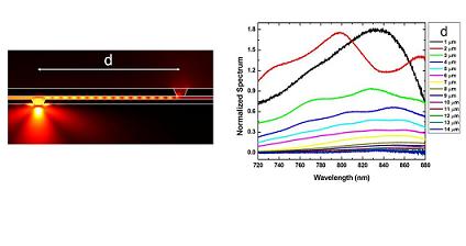 |
| Simulated (left) and experimental (right) coupling of the light emitted by a light-emitting diode (LED) into a MIM waveguide. The left figure shows the electric field profile that results of the coupling of a dipole emitter placed near a subwavelength slit in the bottom layer of the MIM waveguide. The emitted light couples efficiently to the plasmon waveguide mode and results in a standing wave pattern between two slits in the waveguide. This is also measured experimentally, as shown in the spectrally resolved output in the right figure for different lengths between the slits. |
Abstract:
Imec has fabricated electrical sources of surface plasmons, based on integrating light emitting diodes with metal-insulator-metal (MIM) waveguides. These sources, together with earlier work demonstrating plasmon detectors, are a prerequisite for making an interface between electronics and plasmonic circuits. This will lead the way to fully integrated plasmonic biosensing.
Imec demonstrates integrated electrical sources of surface plasmons
Belgium | Posted on June 22nd, 2010Metal-based nanophotonics (plasmonics) is a field concerned with manipulating and focusing light on nanoscale structures that are much smaller than conventional optic components. Plasmonic technology, today still in an experimental stage, has the potential to be used in future applications such as nanoscale optical interconnects for high performance computer chips, highly efficient thin-film solar cells, and extremely sensitive (bio)molecular sensors.
On the nanoscale, incoming light results in surface plasmon polaritons (SPPs), charge density oscillations at metal-dielectric interfaces. These have proven to be excellent markers for biochemical events, because they strongly enhance the local field near metal surfaces or nanostructures, and thus also the specific change induced by the presence of even ultrasmall quantities of biomolecules. Such a detection technique based on surface plasmon resonance (SPR) on thin gold films has already been successfully commercialized. But this technique still uses large external light sources and detectors.
The state of the art in plasmonic waveguides has already been pushed forward substantially during the past years, demonstrating both plasmon propagation in low-loss long-range plasmon waveguides and highly confined plasmon propagation in e.g. metal-dielectric-metal waveguides. However, in order to incorporate such waveguides in realistic integrated circuits, they need to interface with fast and efficient electronics. But to do so, we'd need integrated electrical SPP sources and SPP detectors.
In recent publications in Nano Letters (De Vlaminck, Van Dorpe et al, 2007) and Nature Photonics (Neutens, Van Dorpe et al, 2009), imec has demonstrated the feasibility of efficient integrated detectors of surface plasmons. We have now extended this to integrated electrical sources of surface plasmons based on integrating light emitting diodes with metal-insulator-metal (MIM) waveguides. The strong measured polarization dependence, the experimentally obtained influence of the waveguide length, the measured spectral response are all in line with theoretical expectations. Also surface plasmon polariton interference inside the waveguide is experimentally observed, which allowed us to reliably extract information about the wavelength and confinement of the propagating plasmons (illustrated in the figure). The realization of this building block completes the toolset that is needed to construct truly integrated electrically driven plasmonic circuits and hence paves the way for the integration of nanoscale plasmonic circuitry and integrated plasmonic biosensing.
This work has been published in the highly ranked journal Nano Letters: Neutens et al, Nano Lett. 2010, 10, 1429-1432.
####
About imec
Imec is Europe�s largest independent research center in nanoelectronics and nano-technology. Its staff of more than 1,750 people includes over 550 industrial residents and guest researchers. Imec�s research is applied in better healthcare, smart electronics, sustainable energy, and safer transport.
For more information, please click here
Contacts:
Kapeldreef 75
B-3001 Leuven
Belgium
Phone: +32 16 28 12 11
Fax: +32 16 22 94 00
Copyright © imec
If you have a comment, please Contact us.Issuers of news releases, not 7th Wave, Inc. or Nanotechnology Now, are solely responsible for the accuracy of the content.
Bookmark:


| Related News Press |
News and information
![]() Quantum computer improves AI predictions April 17th, 2026
Quantum computer improves AI predictions April 17th, 2026
![]() Flexible sensor gains sensitivity under pressure April 17th, 2026
Flexible sensor gains sensitivity under pressure April 17th, 2026
![]() A reusable chip for particulate matter sensing April 17th, 2026
A reusable chip for particulate matter sensing April 17th, 2026
![]() Detecting vibrational quantum beating in the predissociation dynamics of SF6 using time-resolved photoelectron spectroscopy April 17th, 2026
Detecting vibrational quantum beating in the predissociation dynamics of SF6 using time-resolved photoelectron spectroscopy April 17th, 2026
Display technology/LEDs/SS Lighting/OLEDs
![]() Spinel-type sulfide semiconductors to operate the next-generation LEDs and solar cells For solar-cell absorbers and green-LED source October 3rd, 2025
Spinel-type sulfide semiconductors to operate the next-generation LEDs and solar cells For solar-cell absorbers and green-LED source October 3rd, 2025
![]() Efficient and stable hybrid perovskite-organic light-emitting diodes with external quantum efficiency exceeding 40 per cent July 5th, 2024
Efficient and stable hybrid perovskite-organic light-emitting diodes with external quantum efficiency exceeding 40 per cent July 5th, 2024
Possible Futures
![]() A fundamentally new therapeutic approach to cystic fibrosis: Nanobody repairs cellular defect April 17th, 2026
A fundamentally new therapeutic approach to cystic fibrosis: Nanobody repairs cellular defect April 17th, 2026
![]() UC Irvine physicists discover method to reverse �quantum scrambling� : The work addresses the problem of information loss in quantum computing system April 17th, 2026
UC Irvine physicists discover method to reverse �quantum scrambling� : The work addresses the problem of information loss in quantum computing system April 17th, 2026
Chip Technology
![]() A reusable chip for particulate matter sensing April 17th, 2026
A reusable chip for particulate matter sensing April 17th, 2026
![]() Metasurfaces smooth light to boost magnetic sensing precision January 30th, 2026
Metasurfaces smooth light to boost magnetic sensing precision January 30th, 2026
Sensors
![]() Flexible sensor gains sensitivity under pressure April 17th, 2026
Flexible sensor gains sensitivity under pressure April 17th, 2026
![]() Tiny nanosheets, big leap: A new sensor detects ethanol at ultra-low levels January 30th, 2026
Tiny nanosheets, big leap: A new sensor detects ethanol at ultra-low levels January 30th, 2026
![]() From sensors to smart systems: the rise of AI-driven photonic noses January 30th, 2026
From sensors to smart systems: the rise of AI-driven photonic noses January 30th, 2026
![]() Sensors innovations for smart lithium-based batteries: advancements, opportunities, and potential challenges August 8th, 2025
Sensors innovations for smart lithium-based batteries: advancements, opportunities, and potential challenges August 8th, 2025
Nanoelectronics
![]() Lab to industry: InSe wafer-scale breakthrough for future electronics August 8th, 2025
Lab to industry: InSe wafer-scale breakthrough for future electronics August 8th, 2025
![]() Interdisciplinary: Rice team tackles the future of semiconductors Multiferroics could be the key to ultralow-energy computing October 6th, 2023
Interdisciplinary: Rice team tackles the future of semiconductors Multiferroics could be the key to ultralow-energy computing October 6th, 2023
![]() Key element for a scalable quantum computer: Physicists from Forschungszentrum J�lich and RWTH Aachen University demonstrate electron transport on a quantum chip September 23rd, 2022
Key element for a scalable quantum computer: Physicists from Forschungszentrum J�lich and RWTH Aachen University demonstrate electron transport on a quantum chip September 23rd, 2022
![]() Reduced power consumption in semiconductor devices September 23rd, 2022
Reduced power consumption in semiconductor devices September 23rd, 2022
Announcements
![]() A fundamentally new therapeutic approach to cystic fibrosis: Nanobody repairs cellular defect April 17th, 2026
A fundamentally new therapeutic approach to cystic fibrosis: Nanobody repairs cellular defect April 17th, 2026
![]() UC Irvine physicists discover method to reverse �quantum scrambling� : The work addresses the problem of information loss in quantum computing system April 17th, 2026
UC Irvine physicists discover method to reverse �quantum scrambling� : The work addresses the problem of information loss in quantum computing system April 17th, 2026
Solar/Photovoltaic
![]() Spinel-type sulfide semiconductors to operate the next-generation LEDs and solar cells For solar-cell absorbers and green-LED source October 3rd, 2025
Spinel-type sulfide semiconductors to operate the next-generation LEDs and solar cells For solar-cell absorbers and green-LED source October 3rd, 2025
![]() KAIST researchers introduce new and improved, next-generation perovskite solar cell November 8th, 2024
KAIST researchers introduce new and improved, next-generation perovskite solar cell November 8th, 2024
![]() Groundbreaking precision in single-molecule optoelectronics August 16th, 2024
Groundbreaking precision in single-molecule optoelectronics August 16th, 2024
![]() Development of zinc oxide nanopagoda array photoelectrode: photoelectrochemical water-splitting hydrogen production January 12th, 2024
Development of zinc oxide nanopagoda array photoelectrode: photoelectrochemical water-splitting hydrogen production January 12th, 2024
|
|
||
|
|
||
| The latest news from around the world, FREE | ||
|
|
||
|
|
||
| Premium Products | ||
|
|
||
|
Only the news you want to read!
Learn More |
||
|
|
||
|
Full-service, expert consulting
Learn More |
||
|
|
||