Home > Press > Nanoscience goes 'big'
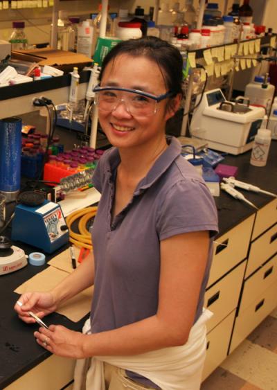 |
| Jen Cha, a UC San Diego nanoengineering professor, is pushing the envelop in nanoscience by using biology to engineer the assembly of nanoscale materials for applications in medicine, electronics and energy. Credit: UC San Diego |
Abstract:
UCSD nanoengineering discovery could lead to enhanced electronics
Nanoscience goes 'big'
San Diego, CA | Posted on January 8th, 2010Nanoscience has the potential to play an enormous role in enhancing a range of products, including sensors, photovoltaics and consumer electronics. Scientists in this field have created a multitude of nano scale materials, such as metal nanocrystals, carbon nanotubes and semiconducting nanowires. However, despite their appeal, it has remained an astounding challenge to engineer the orientation and placement of these materials into the desired device architectures that are reproducible in high yields and at low costs - until now. Jen Cha, a UC San Diego nanoengineering professor, and her team of researchers, have discovered that one way to bridge this gap is to use biomolecules, such as DNA and proteins. Details of this discovery were recently published in a paper titled "Large Area Spatially Ordered Arrays of Gold Nanoparticles Directed by Lithographically Confined DNA Origami," in Nature Nanotechology.
"Self-assembled structures are often too small and affordable lithographic patterns are too large," said Albert Hung, lead author of the Nature Nanotechnology paper and a post doc working in Cha's lab. "But rationally designed synthetic DNA nanostructures allow us to access length scales between 5 and 100 nanometers and bridge the two systems.
"People have created a huge variety of unique and functional nanostructures, but for some intended applications they are worthless unless you can place individual structures, billions or trillions of them at the same time, at precise locations," Hung added. "We hope that our research brings us a step closer to solving this very difficult problem."
Hung said the recently discovered method may be useful for fabricating nanoscale electronic or optical circuits and multiplex sensors.
"A number of groups have worked on parts of this research problem before, but to our knowledge, we're the first to attempt to address so many parts together as a whole," he said.
One of the main applications of this research that Cha and her group are interested in is for sensing. "There is no foreseeable route to be able to build a complex array of different nanoscale sensing elements currently," said Cha, a former IBM research scientist who joined the UCSD Jacobs School of Engineering faculty in 2008. "Our work is one of the first clear examples of how you can merge top down lithography with bottom up self assembly to build such an array. That means that you have a substrate that is patterned by conventional lithography, and then you need to take that pattern and merge it with something that can direct the assembly of even smaller objects, such as those having dimensions between 2 and 20 nanometers. You need an intermediate template, which is the DNA origami, which has the ability to bind to something else much smaller and direct their assembly into the desired configuration. This means we can potentially build transistors from carbon nanotubes and also possibly use nanostructures to detect certain proteins in solutions. Scientists have been talking about patterning different sets of proteins on a substrate and now we have the ability to do that."
Cha said the next step would be to actually develop a device based on this research method.
"I'm very interested in the applications of this research and we're working our way to get there," she said.
For the last 6 years, Cha's research has focused on using biology to engineer the assembly of nanoscale materials for applications in medicine, electronics and energy. One of the limitations of nanoscience is it doesn't allow mass production of products, but Cha's work is focused on trying figure out how to do that and do it cheaply. Much of her recent work has focused on using DNA to build 2D structures.
"Using DNA to assemble materials is an area that many people are excited about," Cha said. "You can fold DNA into anything you want - for example, you can build a large scaffold and within that you could assemble very small objects such as nano particles, nano wires or proteins.
"Engineers need to understand the physical forces needed to build functional arrays from functional materials," she added. "My job as a nanoengineer is to figure out what you need to do to put all the different parts together, whether it's a drug delivery vehicle, photovoltaic applications, sensors or transistors. We need to think about ways to take all the nano materials and engineer them it into something people can use and hold."
Large-area spatially ordered arrays of gold nanoparticles directed by lithographically confined DNA origami, Nature Nanotechnology, Albert M. Hung, Christine M. Micheel, Luisa D. Bozano, Lucas W. Osterbur, Greg M. Wallraff2 & Jennifer N. Cha
####
For more information, please click here
Copyright © Eurekalert
If you have a comment, please Contact us.Issuers of news releases, not 7th Wave, Inc. or Nanotechnology Now, are solely responsible for the accuracy of the content.
Bookmark:


| Related News Press |
News and information
![]() Quantum computer improves AI predictions April 17th, 2026
Quantum computer improves AI predictions April 17th, 2026
![]() Flexible sensor gains sensitivity under pressure April 17th, 2026
Flexible sensor gains sensitivity under pressure April 17th, 2026
![]() A reusable chip for particulate matter sensing April 17th, 2026
A reusable chip for particulate matter sensing April 17th, 2026
![]() Detecting vibrational quantum beating in the predissociation dynamics of SF6 using time-resolved photoelectron spectroscopy April 17th, 2026
Detecting vibrational quantum beating in the predissociation dynamics of SF6 using time-resolved photoelectron spectroscopy April 17th, 2026
Possible Futures
![]() A fundamentally new therapeutic approach to cystic fibrosis: Nanobody repairs cellular defect April 17th, 2026
A fundamentally new therapeutic approach to cystic fibrosis: Nanobody repairs cellular defect April 17th, 2026
![]() UC Irvine physicists discover method to reverse �quantum scrambling� : The work addresses the problem of information loss in quantum computing system April 17th, 2026
UC Irvine physicists discover method to reverse �quantum scrambling� : The work addresses the problem of information loss in quantum computing system April 17th, 2026
Chip Technology
![]() A reusable chip for particulate matter sensing April 17th, 2026
A reusable chip for particulate matter sensing April 17th, 2026
![]() Metasurfaces smooth light to boost magnetic sensing precision January 30th, 2026
Metasurfaces smooth light to boost magnetic sensing precision January 30th, 2026
Self Assembly
![]() Diamond glitter: A play of colors with artificial DNA crystals May 17th, 2024
Diamond glitter: A play of colors with artificial DNA crystals May 17th, 2024
![]() Liquid crystal templated chiral nanomaterials October 14th, 2022
Liquid crystal templated chiral nanomaterials October 14th, 2022
![]() Nanoclusters self-organize into centimeter-scale hierarchical assemblies April 22nd, 2022
Nanoclusters self-organize into centimeter-scale hierarchical assemblies April 22nd, 2022
![]() Atom by atom: building precise smaller nanoparticles with templates March 4th, 2022
Atom by atom: building precise smaller nanoparticles with templates March 4th, 2022
Nanotubes/Buckyballs/Fullerenes/Nanorods/Nanostrings/Nanosheets
![]() Tiny nanosheets, big leap: A new sensor detects ethanol at ultra-low levels January 30th, 2026
Tiny nanosheets, big leap: A new sensor detects ethanol at ultra-low levels January 30th, 2026
![]() Enhancing power factor of p- and n-type single-walled carbon nanotubes April 25th, 2025
Enhancing power factor of p- and n-type single-walled carbon nanotubes April 25th, 2025
![]() Chainmail-like material could be the future of armor: First 2D mechanically interlocked polymer exhibits exceptional flexibility and strength January 17th, 2025
Chainmail-like material could be the future of armor: First 2D mechanically interlocked polymer exhibits exceptional flexibility and strength January 17th, 2025
![]() Innovative biomimetic superhydrophobic coating combines repair and buffering properties for superior anti-erosion December 13th, 2024
Innovative biomimetic superhydrophobic coating combines repair and buffering properties for superior anti-erosion December 13th, 2024
Sensors
![]() Flexible sensor gains sensitivity under pressure April 17th, 2026
Flexible sensor gains sensitivity under pressure April 17th, 2026
![]() Tiny nanosheets, big leap: A new sensor detects ethanol at ultra-low levels January 30th, 2026
Tiny nanosheets, big leap: A new sensor detects ethanol at ultra-low levels January 30th, 2026
![]() From sensors to smart systems: the rise of AI-driven photonic noses January 30th, 2026
From sensors to smart systems: the rise of AI-driven photonic noses January 30th, 2026
![]() Sensors innovations for smart lithium-based batteries: advancements, opportunities, and potential challenges August 8th, 2025
Sensors innovations for smart lithium-based batteries: advancements, opportunities, and potential challenges August 8th, 2025
Nanoelectronics
![]() Lab to industry: InSe wafer-scale breakthrough for future electronics August 8th, 2025
Lab to industry: InSe wafer-scale breakthrough for future electronics August 8th, 2025
![]() Interdisciplinary: Rice team tackles the future of semiconductors Multiferroics could be the key to ultralow-energy computing October 6th, 2023
Interdisciplinary: Rice team tackles the future of semiconductors Multiferroics could be the key to ultralow-energy computing October 6th, 2023
![]() Key element for a scalable quantum computer: Physicists from Forschungszentrum J�lich and RWTH Aachen University demonstrate electron transport on a quantum chip September 23rd, 2022
Key element for a scalable quantum computer: Physicists from Forschungszentrum J�lich and RWTH Aachen University demonstrate electron transport on a quantum chip September 23rd, 2022
![]() Reduced power consumption in semiconductor devices September 23rd, 2022
Reduced power consumption in semiconductor devices September 23rd, 2022
Discoveries
![]() Quantum computer improves AI predictions April 17th, 2026
Quantum computer improves AI predictions April 17th, 2026
![]() Flexible sensor gains sensitivity under pressure April 17th, 2026
Flexible sensor gains sensitivity under pressure April 17th, 2026
![]() A reusable chip for particulate matter sensing April 17th, 2026
A reusable chip for particulate matter sensing April 17th, 2026
![]() Detecting vibrational quantum beating in the predissociation dynamics of SF6 using time-resolved photoelectron spectroscopy April 17th, 2026
Detecting vibrational quantum beating in the predissociation dynamics of SF6 using time-resolved photoelectron spectroscopy April 17th, 2026
Announcements
![]() A fundamentally new therapeutic approach to cystic fibrosis: Nanobody repairs cellular defect April 17th, 2026
A fundamentally new therapeutic approach to cystic fibrosis: Nanobody repairs cellular defect April 17th, 2026
![]() UC Irvine physicists discover method to reverse �quantum scrambling� : The work addresses the problem of information loss in quantum computing system April 17th, 2026
UC Irvine physicists discover method to reverse �quantum scrambling� : The work addresses the problem of information loss in quantum computing system April 17th, 2026
|
|
||
|
|
||
| The latest news from around the world, FREE | ||
|
|
||
|
|
||
| Premium Products | ||
|
|
||
|
Only the news you want to read!
Learn More |
||
|
|
||
|
Full-service, expert consulting
Learn More |
||
|
|
||