Home > Press > Thermochemical nanopatterning of organic semiconductors
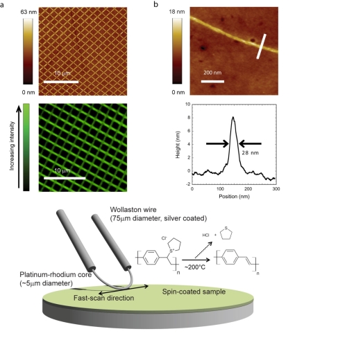 |
| Figure � A schematic of the Wollaston wire probe and the lithographic process (bottom). a Regular patterns drawn over large areas using scanning thermochemical lithography. The top image is an atomic force micrograph, whilst the bottom image is from a confocal microscope. b Atomic force microscope image of a high resolution lithographic line (top) and its cross-section (bottom). |
Abstract:
Researchers from the London Centre for Nanotechnology (LCN) and University College London (UCL) have fabricated sub-30 nm luminescent features of an organic semiconductor via spatially selective conversion and patterning of its precursor by using a heatable, micron-size scanning probe (see figure below). The results will soon be reported in the journal Nature Nanotechnology.
Thermochemical nanopatterning of organic semiconductors
London | Posted on September 8th, 2009The future development of electronics and photonics relies on a range of sophisticated lithographyic techniques for the patterning of semiconducting, dielectric, and metallic materials. Researchers at the London Centre of Nanotechnology (LCN), the Department of Physics and Astronomy, and the Eastman Dental Institute at UCL, have now developed a thermochemical patterning technique for materials known as organic semiconductors.
These materials can be used in light-emitting diodes (LEDs), solar cells, lasers and transistors, and their potential is in low processing costs and the ability to build devices on flexible substrates. However, applications of these materials in nanoelectronics and nanophotonics are limited by the range of patterning techniques available. Many of the approaches to nanolithography that are used to pattern inorganic materials, such as e-beams or Focused Ion Beams (FIBs), are too harsh for organic semiconductors, that can be damaged by the high energy of the patterning beams, or by the chemicals needed for the processing.
So, instead of using standard optical or other "conventional" high-resolution lithographies, the UCL researchers used a small heat source for the patterning. This heat source, known as a modified Wollaston wire, can be mounted on an atomic force microscope and scanned across surfaces to chemically convert all areas it comes into contact with. This technique has allowed the UCL researchers to achieve patterned resolutions below 28 nm and write speeds of 100 �m/s in the widely used organic semiconductor, PPV. The result is particularly surprising given the large diameter of the heat source (5 �m) compared to the resolutions achieved, and since it is likely that resolution could be further improved with the use of nanoscale heat sources, as already reported by other groups.
There has already been some commercial interest in using atomic force microscopes to pattern surfaces, as for example by IBM in their �millipede' project, that was aimed at data-storage applications, but such a thermochemical approach opens up new possibilities. In particular, this work shows that thermochemical lithography offers a versatile, simple and reliable nanopatterning technique. For example, thermo-crosslinkable additives could easily be added to a variety of other solution-processible semiconductors. The technique should also be generally applicable to other classes of materials. A large number of optical materials, including many commercial cross-linker additives and photoresists, rely in fact on chemical mechanisms that can also be thermally activated.
The group, led by Franco Cacialli, has previously used scanning near-field optical lithography (SNOL) for nanopatterning of PPV structures from the same precursor polymer, poly(p-xylene tetrahydrothiophenium chloride) (PXT). This work included the fabrication of quasi-periodic two-dimensional structures with potential for photonic applications. However, the thermochemical technique now developed (Scanning Thermal lithography, or SThL) enables one to bypass the UV insolubilisation step, and the complications and additional costs imposed by the needs for lasers, optics, and sophisticated optical fibre probes.
More details regarding the research in the Organic Semiconductors Group led by Franco Cacialli can be found at the website: www.cmmp.ucl.ac.uk/~fc/OS/
####
About London Centre for Nanotechnology (LCN)
The London Centre for Nanotechnology, LCN, is a UK based multidisciplinary enterprise operating at the forefront of science and technology. It is a joint venture between University College London and Imperial College London and is based at the Bloomsbury and South Kensington sites. It has a unique operating model that accesses and focusses the combined skills of the departments of chemistry, physics, materials, medicine, electrical and electronic engineering, mechanical engineering, chemical engineering, biochemical engineering and earth sciences across the two universities.
For more information, please click here
Contacts:
Bloomsbury (UCL) Site
London Centre for Nanotechnology
17-19 Gordon Street
London WC1H 0AH
tel: +44 (0)20 7679 0604
fax: +44 (0)20 7679 0595
Copyright © London Centre for Nanotechnology (LCN)
If you have a comment, please Contact us.Issuers of news releases, not 7th Wave, Inc. or Nanotechnology Now, are solely responsible for the accuracy of the content.
Bookmark:


| Related News Press |
News and information
![]() Quantum computer improves AI predictions April 17th, 2026
Quantum computer improves AI predictions April 17th, 2026
![]() Flexible sensor gains sensitivity under pressure April 17th, 2026
Flexible sensor gains sensitivity under pressure April 17th, 2026
![]() A reusable chip for particulate matter sensing April 17th, 2026
A reusable chip for particulate matter sensing April 17th, 2026
![]() Detecting vibrational quantum beating in the predissociation dynamics of SF6 using time-resolved photoelectron spectroscopy April 17th, 2026
Detecting vibrational quantum beating in the predissociation dynamics of SF6 using time-resolved photoelectron spectroscopy April 17th, 2026
Display technology/LEDs/SS Lighting/OLEDs
![]() Spinel-type sulfide semiconductors to operate the next-generation LEDs and solar cells For solar-cell absorbers and green-LED source October 3rd, 2025
Spinel-type sulfide semiconductors to operate the next-generation LEDs and solar cells For solar-cell absorbers and green-LED source October 3rd, 2025
![]() Efficient and stable hybrid perovskite-organic light-emitting diodes with external quantum efficiency exceeding 40 per cent July 5th, 2024
Efficient and stable hybrid perovskite-organic light-emitting diodes with external quantum efficiency exceeding 40 per cent July 5th, 2024
Chip Technology
![]() A reusable chip for particulate matter sensing April 17th, 2026
A reusable chip for particulate matter sensing April 17th, 2026
![]() Metasurfaces smooth light to boost magnetic sensing precision January 30th, 2026
Metasurfaces smooth light to boost magnetic sensing precision January 30th, 2026
Nanoelectronics
![]() Lab to industry: InSe wafer-scale breakthrough for future electronics August 8th, 2025
Lab to industry: InSe wafer-scale breakthrough for future electronics August 8th, 2025
![]() Interdisciplinary: Rice team tackles the future of semiconductors Multiferroics could be the key to ultralow-energy computing October 6th, 2023
Interdisciplinary: Rice team tackles the future of semiconductors Multiferroics could be the key to ultralow-energy computing October 6th, 2023
![]() Key element for a scalable quantum computer: Physicists from Forschungszentrum J�lich and RWTH Aachen University demonstrate electron transport on a quantum chip September 23rd, 2022
Key element for a scalable quantum computer: Physicists from Forschungszentrum J�lich and RWTH Aachen University demonstrate electron transport on a quantum chip September 23rd, 2022
![]() Reduced power consumption in semiconductor devices September 23rd, 2022
Reduced power consumption in semiconductor devices September 23rd, 2022
Announcements
![]() A fundamentally new therapeutic approach to cystic fibrosis: Nanobody repairs cellular defect April 17th, 2026
A fundamentally new therapeutic approach to cystic fibrosis: Nanobody repairs cellular defect April 17th, 2026
![]() UC Irvine physicists discover method to reverse �quantum scrambling� : The work addresses the problem of information loss in quantum computing system April 17th, 2026
UC Irvine physicists discover method to reverse �quantum scrambling� : The work addresses the problem of information loss in quantum computing system April 17th, 2026
Tools
![]() Metasurfaces smooth light to boost magnetic sensing precision January 30th, 2026
Metasurfaces smooth light to boost magnetic sensing precision January 30th, 2026
![]() From sensors to smart systems: the rise of AI-driven photonic noses January 30th, 2026
From sensors to smart systems: the rise of AI-driven photonic noses January 30th, 2026
![]() Japan launches fully domestically produced quantum computer: Expo visitors to experience quantum computing firsthand August 8th, 2025
Japan launches fully domestically produced quantum computer: Expo visitors to experience quantum computing firsthand August 8th, 2025
Photonics/Optics/Lasers
![]() Metasurfaces smooth light to boost magnetic sensing precision January 30th, 2026
Metasurfaces smooth light to boost magnetic sensing precision January 30th, 2026
![]() From sensors to smart systems: the rise of AI-driven photonic noses January 30th, 2026
From sensors to smart systems: the rise of AI-driven photonic noses January 30th, 2026
Solar/Photovoltaic
![]() Spinel-type sulfide semiconductors to operate the next-generation LEDs and solar cells For solar-cell absorbers and green-LED source October 3rd, 2025
Spinel-type sulfide semiconductors to operate the next-generation LEDs and solar cells For solar-cell absorbers and green-LED source October 3rd, 2025
![]() KAIST researchers introduce new and improved, next-generation perovskite solar cell November 8th, 2024
KAIST researchers introduce new and improved, next-generation perovskite solar cell November 8th, 2024
![]() Groundbreaking precision in single-molecule optoelectronics August 16th, 2024
Groundbreaking precision in single-molecule optoelectronics August 16th, 2024
![]() Development of zinc oxide nanopagoda array photoelectrode: photoelectrochemical water-splitting hydrogen production January 12th, 2024
Development of zinc oxide nanopagoda array photoelectrode: photoelectrochemical water-splitting hydrogen production January 12th, 2024
|
|
||
|
|
||
| The latest news from around the world, FREE | ||
|
|
||
|
|
||
| Premium Products | ||
|
|
||
|
Only the news you want to read!
Learn More |
||
|
|
||
|
Full-service, expert consulting
Learn More |
||
|
|
||