Home > Press > Team grows nanotubes in one-step process: Discovery may lead to new applications, including biosensors and memory cells
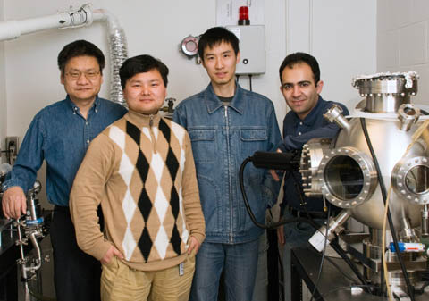 |
| TEAM NANOTUBE - Members of UNL�s Laser Assisted Nano-Technology Lab team who created self-assembling carbon nanotubes are (from left): professor Yongfeng Lu; post-doctoral researcher Yunshen Zhou; and graduate students Wei Xiong and Masoud Mahjouri-Samani. Photo by Greg Nathan/University Communications. |
Abstract:
Scientists and engineers the world over have thought for years that the next generation of smaller, more-efficient electronic and photonic devices could be based on the use of carbon nanotubes, structures 10,000 times thinner than a human hair but with tremendous potential.
Team grows nanotubes in one-step process: Discovery may lead to new applications, including biosensors and memory cells
Lincoln, NE | Posted on February 26th, 2009Using a process based on optical near-field effects, Lu and his team in UNL's Laser Assisted Nano-Engineering Lab created nanoscale devices based on connecting sharp-tipped electrodes with individually self-aligned carbon nanotubes.
Previous efforts in this area by other research groups tried to use advanced instrumentation to manipulate carbon nanotubes after growth. But Lu said that approach is only good for research purposes because it's time consuming and expensive.
"With our method, there's no requirement for expensive instrumentation and no requirement for tedious processes. It's a one-step process," he said. "We call it 'self-aligning growth.' The carbon nanotubes �know' where to start growth.
"In previous efforts, they could only manipulate carbon nanotubes one piece at a time, so they had to align the carbon nanotubes one by one. For our approach using optical near-field effects, all locations with sharp tips can accommodate carbon nanotube growth. That means we can make multiple carbon nanotubes at a time and all of them will be self-aligned."
Nevertheless, the UNL team has not yet been able to produce large numbers of self-aligned carbon nanotubes, but Lu said he and his team see potential for significant expansion that could lead to new applications in devices such as biosensors, light emitters, photon sensors, tiny molecular motors and memory cells.
"We have shown that we can use optical near-field effects to control growth for a small amount of carbon nanotubes," said Lu, Lott professor of electrical engineering at UNL. "We want to make this process scalable so it can be used to make large numbers at a time so we can make a circuit or a system by this approach."
The research was the cover story for the Jan. 14 issue of Nanotechnology, a leading international journal published by the Institute of Physics in the United Kingdom. The research was supported by a grant from the National Science Foundation. Initial funding was provided by the Nebraska Research Initiative.
- Story by By Tom Simons, University Communications
####
For more information, please click here
Copyright © University of Nebraska-Lincoln
If you have a comment, please Contact us.Issuers of news releases, not 7th Wave, Inc. or Nanotechnology Now, are solely responsible for the accuracy of the content.
Bookmark:


| Related News Press |
News and information
![]() Quantum computer improves AI predictions April 17th, 2026
Quantum computer improves AI predictions April 17th, 2026
![]() Flexible sensor gains sensitivity under pressure April 17th, 2026
Flexible sensor gains sensitivity under pressure April 17th, 2026
![]() A reusable chip for particulate matter sensing April 17th, 2026
A reusable chip for particulate matter sensing April 17th, 2026
![]() Detecting vibrational quantum beating in the predissociation dynamics of SF6 using time-resolved photoelectron spectroscopy April 17th, 2026
Detecting vibrational quantum beating in the predissociation dynamics of SF6 using time-resolved photoelectron spectroscopy April 17th, 2026
Chip Technology
![]() A reusable chip for particulate matter sensing April 17th, 2026
A reusable chip for particulate matter sensing April 17th, 2026
![]() Metasurfaces smooth light to boost magnetic sensing precision January 30th, 2026
Metasurfaces smooth light to boost magnetic sensing precision January 30th, 2026
Memory Technology
![]() Researchers tackle the memory bottleneck stalling quantum computing October 3rd, 2025
Researchers tackle the memory bottleneck stalling quantum computing October 3rd, 2025
![]() First real-time observation of two-dimensional melting process: Researchers at Mainz University unveil new insights into magnetic vortex structures August 8th, 2025
First real-time observation of two-dimensional melting process: Researchers at Mainz University unveil new insights into magnetic vortex structures August 8th, 2025
![]() Utilizing palladium for addressing contact issues of buried oxide thin film transistors April 5th, 2024
Utilizing palladium for addressing contact issues of buried oxide thin film transistors April 5th, 2024
Nanoelectronics
![]() Lab to industry: InSe wafer-scale breakthrough for future electronics August 8th, 2025
Lab to industry: InSe wafer-scale breakthrough for future electronics August 8th, 2025
![]() Interdisciplinary: Rice team tackles the future of semiconductors Multiferroics could be the key to ultralow-energy computing October 6th, 2023
Interdisciplinary: Rice team tackles the future of semiconductors Multiferroics could be the key to ultralow-energy computing October 6th, 2023
![]() Key element for a scalable quantum computer: Physicists from Forschungszentrum J�lich and RWTH Aachen University demonstrate electron transport on a quantum chip September 23rd, 2022
Key element for a scalable quantum computer: Physicists from Forschungszentrum J�lich and RWTH Aachen University demonstrate electron transport on a quantum chip September 23rd, 2022
![]() Reduced power consumption in semiconductor devices September 23rd, 2022
Reduced power consumption in semiconductor devices September 23rd, 2022
Discoveries
![]() Quantum computer improves AI predictions April 17th, 2026
Quantum computer improves AI predictions April 17th, 2026
![]() Flexible sensor gains sensitivity under pressure April 17th, 2026
Flexible sensor gains sensitivity under pressure April 17th, 2026
![]() A reusable chip for particulate matter sensing April 17th, 2026
A reusable chip for particulate matter sensing April 17th, 2026
![]() Detecting vibrational quantum beating in the predissociation dynamics of SF6 using time-resolved photoelectron spectroscopy April 17th, 2026
Detecting vibrational quantum beating in the predissociation dynamics of SF6 using time-resolved photoelectron spectroscopy April 17th, 2026
Announcements
![]() A fundamentally new therapeutic approach to cystic fibrosis: Nanobody repairs cellular defect April 17th, 2026
A fundamentally new therapeutic approach to cystic fibrosis: Nanobody repairs cellular defect April 17th, 2026
![]() UC Irvine physicists discover method to reverse �quantum scrambling� : The work addresses the problem of information loss in quantum computing system April 17th, 2026
UC Irvine physicists discover method to reverse �quantum scrambling� : The work addresses the problem of information loss in quantum computing system April 17th, 2026
Photonics/Optics/Lasers
![]() Metasurfaces smooth light to boost magnetic sensing precision January 30th, 2026
Metasurfaces smooth light to boost magnetic sensing precision January 30th, 2026
![]() From sensors to smart systems: the rise of AI-driven photonic noses January 30th, 2026
From sensors to smart systems: the rise of AI-driven photonic noses January 30th, 2026
|
|
||
|
|
||
| The latest news from around the world, FREE | ||
|
|
||
|
|
||
| Premium Products | ||
|
|
||
|
Only the news you want to read!
Learn More |
||
|
|
||
|
Full-service, expert consulting
Learn More |
||
|
|
||