Home > Press > Spin currents: pure and clean: Switching the orientation of magnetization in a thin metallic film can be achieved using the diffusion of electron spin
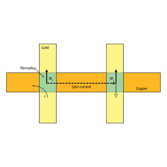 |
| Figure 1: Top view of the device used to switch magnetization using a pure spin current. A current, I, is injected from the gold wire into the permalloy film with magnetization M1. The copper wire creates a spin accumulation at the junction (green). The spin diffuses towards the second junction and can switch the magnetization M2 of the second permalloy film.
Reproduced from Ref. 1 � 2008 Macmillan Publishers Limited |
Abstract:
A team of scientists in Japan has demonstrated the possibility of switching the magnetization of a thin magnetic film with a non-conventional and innovative method, achieving a considerable step forward in magnetic data storage and the field known as spintronics.
Spin currents: pure and clean: Switching the orientation of magnetization in a thin metallic film can be achieved using the diffusion of electron spin
Japan | Posted on February 12th, 2009In magnetic memory devices, information is stored in magnetic elements and typically retrieved by applying a small, external magnetic field. More convenient, however, is the use of a spin-polarized current, in which moving electrons exert a torque on a magnetic element and can switch the direction of its magnetization.
Unfortunately, moving electrons can give rise to electrical noise, which reduces the efficiency of the magnetization control. Now, Yoshichika Otani from the RIKEN Advanced Science Institute in Wako and colleagues have overcome this problem by using a pure spin current1, that is, a diffusion of electron spins without charge motion.
A spin current can be created by the process known as non-local injection: a current is injected into a junction between a metal and a magnetic layer (Fig. 1). When the magnetic element is magnetized, such as a metallic film, electron spins accumulate at the junction, and then diffuse away from the junction to re-equilibrate the spin population in the film. The trick is to then use this spin current to influence the magnetization of another magnetic element placed far from the accumulation point.
Previous attempts to create a pure spin current in this way have all met with limited success. Otani and co-workers therefore focused on optimizing the quality of the interface. In particular, they grew all the layers of their devices in sequence in a single high-vacuum chamber. This prevented possible contamination that could occur while moving a structure between growing chambers.
By examining the electronic transport properties of their device, the researchers were able to demonstrate that when the current injected into the first junction is high enough, it creates a spin current high enough to reverse the magnetization at the second junction. Most importantly, the magnetization can be reversed back by applying the same amount of current in the opposite direction.
Magnetization control using a pure spin current in this way in the high-quality devices fabricated by the team could lead to the realization of very advanced electronic devices. The team believes, for example, that it will be possible to achieve different types of transistors�which have no analogues in current electronics�based only on electron spin.
Reference
1. Yang, T., Kimura, T. & Otani, Y. Giant spin-accumulation signal and pure spin-current-induced reversible magnetization switching. Nature Physics 4, 851-854 (2008).
The corresponding author for this highlight is based at the RIKEN Quantum Nano-Scale Magnetics Team
####
For more information, please click here
Copyright © Riken
If you have a comment, please Contact us.Issuers of news releases, not 7th Wave, Inc. or Nanotechnology Now, are solely responsible for the accuracy of the content.
Bookmark:


| Related Links |
| Related News Press |
News and information
![]() Quantum computer improves AI predictions April 17th, 2026
Quantum computer improves AI predictions April 17th, 2026
![]() Flexible sensor gains sensitivity under pressure April 17th, 2026
Flexible sensor gains sensitivity under pressure April 17th, 2026
![]() A reusable chip for particulate matter sensing April 17th, 2026
A reusable chip for particulate matter sensing April 17th, 2026
![]() Detecting vibrational quantum beating in the predissociation dynamics of SF6 using time-resolved photoelectron spectroscopy April 17th, 2026
Detecting vibrational quantum beating in the predissociation dynamics of SF6 using time-resolved photoelectron spectroscopy April 17th, 2026
Spintronics
![]() Quantum materials: Electron spin measured for the first time June 9th, 2023
Quantum materials: Electron spin measured for the first time June 9th, 2023
Chip Technology
![]() A reusable chip for particulate matter sensing April 17th, 2026
A reusable chip for particulate matter sensing April 17th, 2026
![]() Metasurfaces smooth light to boost magnetic sensing precision January 30th, 2026
Metasurfaces smooth light to boost magnetic sensing precision January 30th, 2026
Memory Technology
![]() Researchers tackle the memory bottleneck stalling quantum computing October 3rd, 2025
Researchers tackle the memory bottleneck stalling quantum computing October 3rd, 2025
![]() First real-time observation of two-dimensional melting process: Researchers at Mainz University unveil new insights into magnetic vortex structures August 8th, 2025
First real-time observation of two-dimensional melting process: Researchers at Mainz University unveil new insights into magnetic vortex structures August 8th, 2025
![]() Utilizing palladium for addressing contact issues of buried oxide thin film transistors April 5th, 2024
Utilizing palladium for addressing contact issues of buried oxide thin film transistors April 5th, 2024
Discoveries
![]() Quantum computer improves AI predictions April 17th, 2026
Quantum computer improves AI predictions April 17th, 2026
![]() Flexible sensor gains sensitivity under pressure April 17th, 2026
Flexible sensor gains sensitivity under pressure April 17th, 2026
![]() A reusable chip for particulate matter sensing April 17th, 2026
A reusable chip for particulate matter sensing April 17th, 2026
![]() Detecting vibrational quantum beating in the predissociation dynamics of SF6 using time-resolved photoelectron spectroscopy April 17th, 2026
Detecting vibrational quantum beating in the predissociation dynamics of SF6 using time-resolved photoelectron spectroscopy April 17th, 2026
Announcements
![]() A fundamentally new therapeutic approach to cystic fibrosis: Nanobody repairs cellular defect April 17th, 2026
A fundamentally new therapeutic approach to cystic fibrosis: Nanobody repairs cellular defect April 17th, 2026
![]() UC Irvine physicists discover method to reverse �quantum scrambling� : The work addresses the problem of information loss in quantum computing system April 17th, 2026
UC Irvine physicists discover method to reverse �quantum scrambling� : The work addresses the problem of information loss in quantum computing system April 17th, 2026
|
|
||
|
|
||
| The latest news from around the world, FREE | ||
|
|
||
|
|
||
| Premium Products | ||
|
|
||
|
Only the news you want to read!
Learn More |
||
|
|
||
|
Full-service, expert consulting
Learn More |
||
|
|
||