Home > Press > Pore-free Ceramics Shine New Light on Lasers, Electronics and Biomedical Implants
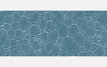 |
| Researchers developed a new class of ceramics that are so pure and perfectly transparent that they can be used as a substitute for crystals in solid-state lasers.
Credit: Dr. Elizabeth Kupp, Adam Stevenson, and Prof. Gary L. Messing, Department of Materials Science and Engineering, The Pennsylvania State University |
Abstract:
To most people, the word "ceramics," refers to opaque clay flower pots or translucent porcelain tea cups. But not all ceramics block or scatter light.
Gary L. Messing, distinguished professor of ceramic science and engineering, and his group at Pennsylvania State University, are developing a brand new class of ceramics that are so pure and perfectly transparent, they can be used as a substitute for crystals in solid-state lasers.
Pore-free Ceramics Shine New Light on Lasers, Electronics and Biomedical Implants
Arlington, VA | Posted on January 31st, 2009Unlike traditional ceramics-such as your favorite coffee mug-materials scientists like Messing focus on what's called advanced ceramics. These have unique mechanical, electrical, optical or thermal properties that make them useful in all sorts of applications.
Advanced ceramics are already used in catalytic converters in cars, protective tiles covering the space shuttle, and electronic components in a desktop computer. In medical applications, advanced ceramics are used as the ball in hip replacements.
There are endless possibilities for taking advantage of the unique qualities of advanced ceramics. Many applications are limited, however, by tiny holes, called pores, which scatter light and make them opaque or translucent. Pores can also make the ceramic too brittle and ruin the flow of electrons and /or heat through the material.
"As a result of advances in ceramic processing science, we can now produce extremely high purity ceramics with almost no defects or pores," Messing said.
How "perfect" are the new ceramics? Messing and co-author Adam J. Stevenson reported a new method of making ceramic crystals that are over 99.999 percent free of pores, in their recent article, "Toward Pore-Free Ceramics," published in the Oct. 17, 2008, edition of Science.
At this level of density, there are usually only a few hundred tiny pores left in the researchers' samples after processing. And those pores that remain are generally only 10 to a few hundred nanometers in diameter-about five times smaller than the width of a human hair.
To make such dense ceramics, the scientists use synthetic powders, because they are much purer than clays and other materials mined from the earth. "We start with a very fine powder, form that powder into a desired shape, and then heat the formed powder to create a solid, dense body," said Messing.
This heating process, called sintering, happens at temperatures below the material's melting point. So without liquefying the material, sintering allows atoms in the powder to move around and fill in the spaces between the individual grains.
Soap-bubble Ceramics
"As we sinter a ceramic, the average size of the grains increases, because the larger grains slowly consume the smaller grains," said Messing. "You can visualize this process at home by making soap bubbles in the sink. If you watch carefully, the larger bubbles in the foam will absorb the smaller bubbles."
According to Messing, soap bubble observations like these actually helped materials scientists figure out some aspects of creating ceramics decades ago. "The physics behind 'grain growth' in both soap bubbles and ceramics are identical," he said. "It just happens on a much smaller scale and at higher temperatures in ceramics."
Some scientists predict that different properties of advanced ceramics may be enhanced by reducing grains to nanometer size. "Unfortunately, it can be difficult to make materials this small," said Messing. "If we understand the processes that lead to grain growth better, we can refine the grain size to the nanoscale and maximize mechanical, electrical and optical properties of the ceramic material."
Ceramic Lasers
To test their new method, Messing and his group made neodymium-doped yttrium aluminum garnet (Nd:YAG) laser ceramics, because they are important in industrial and military applications. The Nd:YAG crystal structure also works well with ceramic processing.
"Most high power, solid-state lasers use single crystals made by melt-growth methods," said Stevenson. "These require high temperatures of greater than 1950 degrees Celsius, and weeks or months to grow a single crystal boule [block] of Nd:YAG."
According to Stevenson, switching to ceramic processing could reduce the temperatures needed to make an Nd:YAG laser ceramic by at least 250 degrees Celsius and reduce the time it takes down to just days.
To make the ceramics, the group started with powders and mixed them with liquids and polymers to make a material similar in consistency to paint. "We used a process called tape casting to make long thin sheets of the material," Messing explained. "Next, we cut the sheets into squares and stacked them to form thicker squares about 1 centimeter x 5 cm x 5 cm."
After applying heat to sinter the squares, the ceramics became transparent. But the material still contained enough pores to degrade a laser's performance.
"We did a final step, called hot isostatic pressing (HIP), where we heated the ceramics to over 1600 degrees Celsius and applied high pressures with argon gas," Messing said. "By combining heat with pressure, we eliminated the few remaining pores."
Future Ceramics
After sintering and HIP, a ceramic material looks like a mosaic of tiny crystals, almost like a puzzle, when viewed under a scanning electron microscope.
"The presence of grain boundaries, or junctions, between individual crystals is the single most important difference between melt-grown single crystals and perfect ceramics," Messing said. "But we believe that the grain boundaries are so small that they have virtually no effect on the light traveling through the material."
Studying the effects of grain boundaries on transparent ceramics is just one area the researchers will pursue in the future. "Ceramics can eliminate most of the inherent defects of melt-grown crystals," Messing believes. "That means we may be able to make ceramics with superior optical properties."
For example, by controlling the positions of the ions inside the ceramic, scientists may be able to create new designs for high power lasers. And ceramic processing could allow complex shaped parts, using extrusion or slip casting, for novel laser designs-something they could never achieve with melt-grown crystals.
"Our goals are to make perfect materials and to lay out the science of transparent ceramics in such a way that it can easily be applied to other systems in the future," Stevenson said.
"Although we have made a number of innovations, and we use a number of novel processes, what we do is basic ceramic processing," he said. "The key to achieving transparency is reaching a level of perfection at each stage of the process, which most applications do not require."
"Theory and computational modeling are needed to understand how to shrink pores and limit grain growth," said NSF program director Lynnette Madsen. "And we are in desperate need for tools to monitor nanometer-size pores and grains during the final stage of the sintering process."
According to Madsen, advances such as these will lead to the development of better techniques for making bulk, nanostructured ceramics. "Not only will this research have a positive impact on many essential applications, it will alter how materials science is taught to students," she said.
Investigators
Gary Messing
Adam Stevenson
Venkatraman Gopalan
Related Institutions/Organizations
Pennsylvania State Univ University Park
####
About National Science Foundation
The National Science Foundation (NSF) is an independent federal agency that supports fundamental research and education across all fields of science and engineering, with an annual budget of $5.92 billion. NSF funds reach all 50 states through grants to over 1,700 universities and institutions. Each year, NSF receives about 42,000 competitive requests for funding, and makes over 10,000 new funding awards. The NSF also awards over $400 million in professional and service contracts yearly.
For more information, please click here
Contacts:
Holly Martin
National Science Foundation
Copyright © National Science Foundation
If you have a comment, please Contact us.Issuers of news releases, not 7th Wave, Inc. or Nanotechnology Now, are solely responsible for the accuracy of the content.
Bookmark:


| Related News Press |
News and information
![]() Quantum computer improves AI predictions April 17th, 2026
Quantum computer improves AI predictions April 17th, 2026
![]() Flexible sensor gains sensitivity under pressure April 17th, 2026
Flexible sensor gains sensitivity under pressure April 17th, 2026
![]() A reusable chip for particulate matter sensing April 17th, 2026
A reusable chip for particulate matter sensing April 17th, 2026
![]() Detecting vibrational quantum beating in the predissociation dynamics of SF6 using time-resolved photoelectron spectroscopy April 17th, 2026
Detecting vibrational quantum beating in the predissociation dynamics of SF6 using time-resolved photoelectron spectroscopy April 17th, 2026
Chip Technology
![]() A reusable chip for particulate matter sensing April 17th, 2026
A reusable chip for particulate matter sensing April 17th, 2026
![]() Metasurfaces smooth light to boost magnetic sensing precision January 30th, 2026
Metasurfaces smooth light to boost magnetic sensing precision January 30th, 2026
Nanomedicine
![]() A fundamentally new therapeutic approach to cystic fibrosis: Nanobody repairs cellular defect April 17th, 2026
A fundamentally new therapeutic approach to cystic fibrosis: Nanobody repairs cellular defect April 17th, 2026
![]() New molecular technology targets tumors and simultaneously silences two �undruggable� cancer genes August 8th, 2025
New molecular technology targets tumors and simultaneously silences two �undruggable� cancer genes August 8th, 2025
![]() New imaging approach transforms study of bacterial biofilms August 8th, 2025
New imaging approach transforms study of bacterial biofilms August 8th, 2025
![]() Electrifying results shed light on graphene foam as a potential material for lab grown cartilage June 6th, 2025
Electrifying results shed light on graphene foam as a potential material for lab grown cartilage June 6th, 2025
Discoveries
![]() Quantum computer improves AI predictions April 17th, 2026
Quantum computer improves AI predictions April 17th, 2026
![]() Flexible sensor gains sensitivity under pressure April 17th, 2026
Flexible sensor gains sensitivity under pressure April 17th, 2026
![]() A reusable chip for particulate matter sensing April 17th, 2026
A reusable chip for particulate matter sensing April 17th, 2026
![]() Detecting vibrational quantum beating in the predissociation dynamics of SF6 using time-resolved photoelectron spectroscopy April 17th, 2026
Detecting vibrational quantum beating in the predissociation dynamics of SF6 using time-resolved photoelectron spectroscopy April 17th, 2026
Materials/Metamaterials/Magnetoresistance
![]() First real-time observation of two-dimensional melting process: Researchers at Mainz University unveil new insights into magnetic vortex structures August 8th, 2025
First real-time observation of two-dimensional melting process: Researchers at Mainz University unveil new insights into magnetic vortex structures August 8th, 2025
![]() Researchers unveil a groundbreaking clay-based solution to capture carbon dioxide and combat climate change June 6th, 2025
Researchers unveil a groundbreaking clay-based solution to capture carbon dioxide and combat climate change June 6th, 2025
![]() A 1960s idea inspires NBI researchers to study hitherto inaccessible quantum states June 6th, 2025
A 1960s idea inspires NBI researchers to study hitherto inaccessible quantum states June 6th, 2025
![]() Institute for Nanoscience hosts annual proposal planning meeting May 16th, 2025
Institute for Nanoscience hosts annual proposal planning meeting May 16th, 2025
Announcements
![]() A fundamentally new therapeutic approach to cystic fibrosis: Nanobody repairs cellular defect April 17th, 2026
A fundamentally new therapeutic approach to cystic fibrosis: Nanobody repairs cellular defect April 17th, 2026
![]() UC Irvine physicists discover method to reverse �quantum scrambling� : The work addresses the problem of information loss in quantum computing system April 17th, 2026
UC Irvine physicists discover method to reverse �quantum scrambling� : The work addresses the problem of information loss in quantum computing system April 17th, 2026
Photonics/Optics/Lasers
![]() Metasurfaces smooth light to boost magnetic sensing precision January 30th, 2026
Metasurfaces smooth light to boost magnetic sensing precision January 30th, 2026
![]() From sensors to smart systems: the rise of AI-driven photonic noses January 30th, 2026
From sensors to smart systems: the rise of AI-driven photonic noses January 30th, 2026
|
|
||
|
|
||
| The latest news from around the world, FREE | ||
|
|
||
|
|
||
| Premium Products | ||
|
|
||
|
Only the news you want to read!
Learn More |
||
|
|
||
|
Full-service, expert consulting
Learn More |
||
|
|
||