Home > Press > The Brightest, Sharpest, Fastest X-Ray Holograms Yet
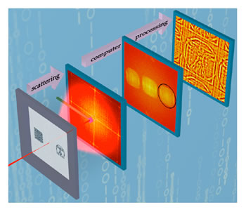 |
| A coherent x-ray beam illuminates both the sample and a uniformly redundant array (URA) placed next to it. The CCD detector (whose center is shielded from the direct beam) collects diffracted x-rays from both sample and URA. Processing the resulting interference patterns subsequently yields a hologram. |
Abstract:
The pinhole camera, a technique known since ancient times, has inspired a futuristic technology for lensless, three-dimensional imaging. Working at both the Advanced Light Source (ALS) at the U.S. Department of Energy's Lawrence Berkeley National Laboratory, and at FLASH, the free-electron laser in Hamburg, Germany, an international group of scientists has produced two of the brightest, sharpest x-ray holograms of microscopic objects ever made, thousands of times more efficiently than previous x-ray-holographic methods.
The Brightest, Sharpest, Fastest X-Ray Holograms Yet
BERKELEY, CA | Posted on August 2nd, 2008The x-ray hologram made at ALS beamline 9.0.1 was of Leonardo da Vinci's famous drawing, "Vitruvian Man," a lithographic reproduction less than two micrometers (millionths of a meter, or microns) square, etched with an electron-beam nanowriter. The hologram required a five-second exposure and had a resolution of 50 nanometers (billionths of a meter).
The other hologram, made at FLASH, was of a single bacterium, Spiroplasma milliferum, made at 150-nanometer resolution and computer-refined to 75 nanometers, but requiring an exposure to the beam of just 15 femtoseconds (quadrillionths of a second).
The values for these two holograms are among the best ever reported for micron-sized objects. With already established technologies, resolutions obtained by these methods could be pushed to only a few nanometers, or, using computer refinement, even better.
The researchers were from Berkeley Lab; Lawrence Livermore National Laboratory; the Stanford Linear Accelerator Center; Uppsala University, Sweden; the University of Hamburg and the Deutsches Elektronen-Synchrotron (DESY), Germany; Arizona State University; Princeton University; and the University of California at Berkeley. Their results appear in advanced online publication of Nature Photonics, available online to subscribers at www.nature.com/nphoton/index.html.
The modern pinhole camera
"Our purpose was to explore methods of making images of nanoscale objects on the time scale of atomic motions, a length and time regime that promises to become accessible with advances in free-electron lasers," says Stefano Marchesini of the ALS, who led the research. "The technique we used is called massively parallel x-ray Fourier-transform holography, with �coded apertures.' What inspired me to try this approach was the pinhole camera."
The ancient Greeks made note of pinhole-camera effects without understanding them; later, pinhole cameras were used by Chinese, Arab, and European scholars. Renaissance painters learned the principals of perspective using the camera obscura, literally a "dark room," with a pinhole in one wall that projected the outside scene onto the opposite wall.
"The room had to be dark for the good reason that a sharp image requires a small pinhole, but a small pinhole also produces a dim image," says Marchesini. "To get a brighter image without lenses you have to use many pinholes. The problem then becomes how to assemble the information, including depth information, from the overlapping shadow images. This is where �coded apertures' come in."
By knowing the precise layout of a pinhole array, including the different sizes of the different pinholes, a computer can recover a bright, high-resolution image numerically. Random pinhole arrays were first used in x-ray astronomy but soon evolved into regular rows and columns of tiny square apertures of varying dimension. These coded apertures are called uniformly redundant arrays, or URAs.
Marchesini knew that colleagues at Livermore were using URAs in gamma-ray detectors. He asked himself, "What would happen if we put a URA right next to an object we were imaging with the x-ray beamline? It should allow us to create a holographic image - one with orders of magnitude more intensity than a standard hologram."
Holography with x-rays
Holography was invented over 60 years ago by the physicist Dennis Gabor, but its use has long been limited by technology. Whereas a pinhole camera employs ray optics, in which the photons travel like a stream of particles, holography depends on the wave-like properties of light.
The principle is straightforward: a beam of light illuminates an object, which scatters the light onto a detector such as a photographic plate. Meanwhile a second, identical beam of light shines directly on the detector. The scattered light waves from the object beam form interference patterns with the unscattered light waves from the reference beam.
This interference pattern serves to reconstruct an image of the object. One easy way to do so, if the detector is a photo transparency, is for the observer to look through the transparency in the direction of the (now absent) object; if only the reference beam is shining on the detector, the interference pattern serves to "unscatter" (diffract) the wavefront and reconstruct the object's image.
Lasers, which produce coherent light (all the same phase) were the first invention that made holography practical; it is now possible to make small holograms using just a laser pointer. FLASH is a powerful free-electron laser (FEL); a new generation of FELs of much shorter wavelength will be capable of producing coherent light pulses so short they'll be able to freeze atomic motion in the midst of chemical reactions.
Soft x-rays like those from ALS beamline 9.0.1 can also be made coherent, or laser-like, using a pair of pinholes. (The beam is conditioned by these pinholes, but they are not directly involved in imaging, except to make the beam laser-like.) To make a hologram, the beam issuing from the synchrotron scatters from the target object and is collected on a CCD detector. Meanwhile the same beam simultaneously passes through the multiple-"pinhole" URA, mounted on the same plate as the target object, and produces a bright reference beam.
The scattered image of the object and the many overlapping reference beams from the URA combine to make an interference pattern which contains all the information, including the relative depth of individual features, needed to mathematically reconstruct a three-dimensional image of the object.
The hologram of the Spiroplasma bacterium was made in precisely the same way, with much brighter x-ray beams and a much shorter pulse of light. So bright was the flash of light that the sample was vaporized, but not before both the scattered object beam and the reference beams from the URA had been recorded.
Together, the two experiments demonstrate that holographic x-ray images with nanometer-scale resolution can be made of objects measured in microns, in times as brief as femtoseconds. Moreover, sample preparation time is fast and easily repeated for high throughput during repetitive experiments. As the researchers write in their Nature Photonics article, "Imaging with coherent x-rays will be a key technique for developing nanoscience and nanotechnology, and massively parallel holography will be an enabling tool in this quest."
"Massively parallel x-ray holography," by Stefano Marchesini, S�bastien Boutet, Anne E. Sakdinawat, Michael J. Bogan, Sǎsa Bajt, Anton Barty, Henry N. Chapman, Matthias Frank, Stefan P. Hau-Riege, Abraham Sz�ke, Congwu Cui, David Shapiro, Malcolm Howells, John Spence, Joshua Shaevitz, Joanna Lee, Janos Hajdu, and Marvin M. Siebert, appears in advanced online publication of Nature Photonics and is available online to subscribers at http://www.nature.com/nphoton/index.html.
This work was supported by grants from the U.S. Department of Energy, the European Union, the Swedish Research Councils, the Munich Centre for Advanced Photonics, the Natural Sciences and Engineering Research Council of Canada, and the Sven and Lilly Lawskis Foundation.
####
About Berkeley Lab
Berkeley Lab is a U.S. Department of Energy national laboratory located in Berkeley, California. It conducts unclassified scientific research and is managed by the University of California.
For more information, please click here
Contacts:
Paul Preuss
(510) 486-6249
Copyright © Berkeley Lab
If you have a comment, please Contact us.Issuers of news releases, not 7th Wave, Inc. or Nanotechnology Now, are solely responsible for the accuracy of the content.
Bookmark:


| Related News Press |
News and information
![]() Quantum computer improves AI predictions April 17th, 2026
Quantum computer improves AI predictions April 17th, 2026
![]() Flexible sensor gains sensitivity under pressure April 17th, 2026
Flexible sensor gains sensitivity under pressure April 17th, 2026
![]() A reusable chip for particulate matter sensing April 17th, 2026
A reusable chip for particulate matter sensing April 17th, 2026
![]() Detecting vibrational quantum beating in the predissociation dynamics of SF6 using time-resolved photoelectron spectroscopy April 17th, 2026
Detecting vibrational quantum beating in the predissociation dynamics of SF6 using time-resolved photoelectron spectroscopy April 17th, 2026
Imaging
![]() Simple algorithm paired with standard imaging tool could predict failure in lithium metal batteries August 8th, 2025
Simple algorithm paired with standard imaging tool could predict failure in lithium metal batteries August 8th, 2025
![]() First real-time observation of two-dimensional melting process: Researchers at Mainz University unveil new insights into magnetic vortex structures August 8th, 2025
First real-time observation of two-dimensional melting process: Researchers at Mainz University unveil new insights into magnetic vortex structures August 8th, 2025
![]() New imaging approach transforms study of bacterial biofilms August 8th, 2025
New imaging approach transforms study of bacterial biofilms August 8th, 2025
Laboratories
![]() Researchers develop molecular qubits that communicate at telecom frequencies October 3rd, 2025
Researchers develop molecular qubits that communicate at telecom frequencies October 3rd, 2025
Govt.-Legislation/Regulation/Funding/Policy
![]() Quantum computer improves AI predictions April 17th, 2026
Quantum computer improves AI predictions April 17th, 2026
![]() Metasurfaces smooth light to boost magnetic sensing precision January 30th, 2026
Metasurfaces smooth light to boost magnetic sensing precision January 30th, 2026
![]() New imaging approach transforms study of bacterial biofilms August 8th, 2025
New imaging approach transforms study of bacterial biofilms August 8th, 2025
Discoveries
![]() Quantum computer improves AI predictions April 17th, 2026
Quantum computer improves AI predictions April 17th, 2026
![]() Flexible sensor gains sensitivity under pressure April 17th, 2026
Flexible sensor gains sensitivity under pressure April 17th, 2026
![]() A reusable chip for particulate matter sensing April 17th, 2026
A reusable chip for particulate matter sensing April 17th, 2026
![]() Detecting vibrational quantum beating in the predissociation dynamics of SF6 using time-resolved photoelectron spectroscopy April 17th, 2026
Detecting vibrational quantum beating in the predissociation dynamics of SF6 using time-resolved photoelectron spectroscopy April 17th, 2026
Announcements
![]() A fundamentally new therapeutic approach to cystic fibrosis: Nanobody repairs cellular defect April 17th, 2026
A fundamentally new therapeutic approach to cystic fibrosis: Nanobody repairs cellular defect April 17th, 2026
![]() UC Irvine physicists discover method to reverse �quantum scrambling� : The work addresses the problem of information loss in quantum computing system April 17th, 2026
UC Irvine physicists discover method to reverse �quantum scrambling� : The work addresses the problem of information loss in quantum computing system April 17th, 2026
Photonics/Optics/Lasers
![]() Metasurfaces smooth light to boost magnetic sensing precision January 30th, 2026
Metasurfaces smooth light to boost magnetic sensing precision January 30th, 2026
![]() From sensors to smart systems: the rise of AI-driven photonic noses January 30th, 2026
From sensors to smart systems: the rise of AI-driven photonic noses January 30th, 2026
Research partnerships
![]() Lab to industry: InSe wafer-scale breakthrough for future electronics August 8th, 2025
Lab to industry: InSe wafer-scale breakthrough for future electronics August 8th, 2025
![]() HKU physicists uncover hidden order in the quantum world through deconfined quantum critical points April 25th, 2025
HKU physicists uncover hidden order in the quantum world through deconfined quantum critical points April 25th, 2025
|
|
||
|
|
||
| The latest news from around the world, FREE | ||
|
|
||
|
|
||
| Premium Products | ||
|
|
||
|
Only the news you want to read!
Learn More |
||
|
|
||
|
Full-service, expert consulting
Learn More |
||
|
|
||