Home > Press > Nano-layer of Ruthenium Stabilizes Magnetic Sensors
 |
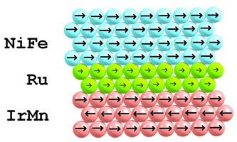
| A thin layer of ruthenium (green in the cartoon) improves magnetic sensors by modulating interactions between a nickel/iron film (blue) that responds to external magnetic fields and an iridium/manganese stabilizer film (pink). The ruthenium aligns its electron spins, indicated by arrows, with the nearest layers in both films.
Credit: NIST |
Abstract:
A layer of ruthenium just a few atoms thick can be used to fine-tune the sensitivity and enhance the reliability of magnetic sensors, tests at the National Institute of Standards and Technology (NIST) show.* The nonmagnetic metal acts as a buffer between active layers of sensor materials, offering a simple means of customizing field instruments such as compasses, and stabilizing the magnetization in a given direction in devices such as computer hard-disk readers.
Nano-layer of Ruthenium Stabilizes Magnetic Sensors
GAITHERSBURG, MD | Posted on August 3rd, 2007n the NIST sensor design, ruthenium modulates interactions between a ferromagnetic film (in which electron "spins" all point in the same direction) and an antiferromagnetic film (in which different layers of electrons point in opposite directions to stabilize the device). In the presence of a magnetic field, the electron spins in the ferromagnetic film rotate, changing the sensor's resistance and producing a voltage output. The antiferromagnetic film, which feels no force because it has no net magnetization, acts like a very stiff spring that resists the rotation and stabilizes the sensor. The ruthenium layer (see graphic) is added to weaken the spring, effectively making the device more sensitive. This makes it easier to rotate the electron spins, and still pulls them back to their original direction when the field is removed.
NIST tests showed that thicker buffers of ruthenium (up to 2 nanometers) make it easier to rotate the magnetization of the ferromagnetic film, resulting in a more sensitive device. Thinner buffers result in a device that is less sensitive but responds to a wider range of external fields. Ruthenium layers thicker than 2 nm prevent any coupling between the two active films. All buffer thicknesses from 0 to 2 nm maintain sensor magnetization (even resetting it if necessary) without a boost from an external electrical current or magnetic field. This easily prevents demagnetization and failure of a sensor.
The mass-producible test sensors, made in the NIST clean room in Boulder, Colo., consist of three basic layers of material deposited on silicon wafers: The bottom antiferromagnetic layer is 8 nm of an iridium/manganese alloy, followed by the ruthenium buffer, and topped with 25 nm of a nickel/iron alloy. The design requires no extra lithography steps for the magnetic layers and could be implemented in existing mass-production processes. By contrast, the conventional method of modulating magnetoresistive sensors�capping the ends of sensors with magnetic materials�adds fabrication steps and does not allow fine-tuning of sensitivity. The new sensor design was key to NIST's recent development of a high-resolution forensic tape analysis system for the Federal Bureau of Investigation (see Magnetic Tape Analysis "Sees" Tampering in Detail).
http://www.nist.gov/public_affairs/techbeat/tb2007_0720.htm#tape
* S.T. Halloran, F.C. da Silva, H.Z. Fardi and D.P. Pappas. Permanent-magnet-free stabilization and sensitivity tailoring of magneto-resistive field sensors, Journal of Applied Physics. August 1, 2007.
####
About NIST
Founded in 1901, NIST is a non-regulatory federal agency within the U.S. Commerce Department's Technology Administration. NIST's mission is to promote U.S. innovation and industrial competitiveness by advancing measurement science, standards, and technology in ways that enhance economic security and improve our quality of life.
For more information, please click here
Contacts:
Laura Ost
(303) 497-4880
Copyright © NIST
If you have a comment, please Contact us.Issuers of news releases, not 7th Wave, Inc. or Nanotechnology Now, are solely responsible for the accuracy of the content.
| Related News Press |
Sensors
![]() Flexible sensor gains sensitivity under pressure April 17th, 2026
Flexible sensor gains sensitivity under pressure April 17th, 2026
![]() Tiny nanosheets, big leap: A new sensor detects ethanol at ultra-low levels January 30th, 2026
Tiny nanosheets, big leap: A new sensor detects ethanol at ultra-low levels January 30th, 2026
![]() From sensors to smart systems: the rise of AI-driven photonic noses January 30th, 2026
From sensors to smart systems: the rise of AI-driven photonic noses January 30th, 2026
![]() Sensors innovations for smart lithium-based batteries: advancements, opportunities, and potential challenges August 8th, 2025
Sensors innovations for smart lithium-based batteries: advancements, opportunities, and potential challenges August 8th, 2025
Announcements
![]() A fundamentally new therapeutic approach to cystic fibrosis: Nanobody repairs cellular defect April 17th, 2026
A fundamentally new therapeutic approach to cystic fibrosis: Nanobody repairs cellular defect April 17th, 2026
![]() UC Irvine physicists discover method to reverse �quantum scrambling� : The work addresses the problem of information loss in quantum computing system April 17th, 2026
UC Irvine physicists discover method to reverse �quantum scrambling� : The work addresses the problem of information loss in quantum computing system April 17th, 2026
|
|
||
|
|
||
| The latest news from around the world, FREE | ||
|
|
||
|
|
||
| Premium Products | ||
|
|
||
|
Only the news you want to read!
Learn More |
||
|
|
||
|
Full-service, expert consulting
Learn More |
||
|
|
||


