Home > Press > TUS researchers propose a simple, inexpensive approach to fabricating carbon nanotube wiring on plastic films: The proposed method produces wiring suitable for developing all-carbon devices, including flexible sensors and energy conversion and storage devices
 |
| A novel method proposed by TUS researchers for the fabrication of multi-walled carbon nanotubes on flexible substrates, such as plastic films, eliminates many of the drawbacks of conventional techniques and can be used to mass-produce carbon wiring for flexible all-carbon electronic devices. CREDIT Takashi Ikuno from TUS, Japan |
Abstract:
Carbon nanotubes (CNTs) are cylindrical tube-like structures made of carbon atoms that display highly desirable physical properties like high strength, low weight, and excellent thermal and electrical conductivities. This makes them ideal materials for various applications, including reinforcement materials, energy storage and conversion devices, and electronics. Despite such immense potential, however, there have been challenges in commercializing CNTs, such as their incorporation on plastic substrates for fabricating flexible CNT-based devices. Traditional fabrication methods require carefully controlled environments such as high temperatures and a clean room. Further, they require repeat transfers to produce CNTs with different resistance values.
TUS researchers propose a simple, inexpensive approach to fabricating carbon nanotube wiring on plastic films: The proposed method produces wiring suitable for developing all-carbon devices, including flexible sensors and energy conversion and storage devices
Tokyo, Japan | Posted on March 3rd, 2023More direct methods such as laser-induced forward transfer (LIFT) and thermal fusion (TF) have been developed as alternatives. In the LIFT method, a laser is used to directly transfer CNTs onto substrates, while in TF, CNTs are mixed with polymers that are then selectively removed by a laser to form CNT wires with varying resistance values. However, both these methods are expensive and have their unique problems. LIFT requires expensive pulsed lasers and preparation of CNTs with specific resistance values, while TF uses large amounts of CNTs that are not utilized and go to waste.
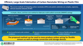
Aiming to develop a more simple and inexpensive approach, Associate Professor Dr. Takashi Ikuno along with his collaborators, Mr. Hiroaki Komatsu, Mr. Yosuke Sugita and Mr. Takahiro Matsunami at Tokyo University of Science, Japan, recently proposed a novel method that enables fabrication of multi-walled CNT (MWNT) wiring on a plastic film under ambient conditions (room temperature and atmospheric pressure) using a low-cost laser.
The breakthrough, published in the journal Scientific Reports on 08 February 2023, involves coating a polypropylene (PP) film with an MWNT film about 10 μm thick and then exposing it to a mW UV laser. The result is a conductive wiring made of a combination of MWNT and PP.
�This process enables the easy �drawing� of wiring and flexible devices for wearable sensors without the need for complex processes,� highlights Dr. Ikuno.
The researchers attributed the formation of these wires to the difference in the thermal conductivities between the MWNT and the PP film. As the MWNT/PP film is exposed to the laser, the high thermal conductivity of the MWNT layer causes the heat to spread along the length of the wire, resulting in high temperatures at the MWNT�PP interface and lower temperatures elsewhere in the PP film. Directly below the laser, where temperatures are the highest, the PP diffuses into the MWNT film to form a thick PP/MWNT composite, while a thin PP/MWNT layer is formed at the edges of the laser where temperatures are relatively low.
The proposed method also allows the fabrication of carbon wires with different resistance values within the same process (without repeat transfer) by simply changing the irradiation conditions, thereby eliminating the need for additional steps. Exposing the PP/MWNT film to high laser energies, achieved either by low scanning speeds, a high number of laser exposures, or the use of a high-powered laser, produces thicker wires with a higher concentration of MWNTs. Consequently, the lower resistivity of MWNT and the thicker wire lowers the resistance per unit length of the wire (resistance is directly proportional to the ratio between the resistivity and the thickness of the wire).
By precisely controlling the exposure of the MWNT/PP film to laser light, the researchers successfully fabricated MWNT wires with a wide range of resistance values, from 0.789 kΩ/cm to 114 kΩ/cm. Moreover, these wires were highly flexible and maintained their resistance even when bent repeatedly.
Additionally, the method solved one of the pressing issues with current techniques, namely the inability of LIFT and TF techniques to reuse CNTs not utilized in the fabrication process. In the proposed method, MWNTs not incorporated into the PP film during laser irradiation can be recovered and reused, allowing for the creation of new MWNT wires with little to no change in resistance values.
With its simplicity, efficient utilization of CNTs, and the capability to create high-quality wires, the new method has the potential to realize large-scale manufacturing of flexible carbon wiring for flexible sensors and energy conversion and storage devices.
�We expect the process cost to be significantly reduced compared to that for conventional methods. This, in turn, will contribute to the realization of low-cost flexible sensors that are expected to have wide applications in large quantities,� concludes Dr. Ikuno.
####
About Tokyo University of Science
Tokyo University of Science (TUS) is a well-known and respected university, and the largest science-specialized private research university in Japan, with four campuses in central Tokyo and its suburbs and in Hokkaido. Established in 1881, the university has continually contributed to Japan's development in science through inculcating the love for science in researchers, technicians, and educators.
With a mission of �Creating science and technology for the harmonious development of nature, human beings, and society,� TUS has undertaken a wide range of research from basic to applied science. TUS has embraced a multidisciplinary approach to research and undertaken intensive study in some of today's most vital fields. TUS is a meritocracy where the best in science is recognized and nurtured. It is the only private university in Japan that has produced a Nobel Prize winner and the only private university in Asia to produce Nobel Prize winners within the natural sciences field.
Website: https://www.tus.ac.jp/en/mediarelations/
About Associate Professor Takashi Ikuno from Tokyo University of Science
Takashi Ikuno received his Ph.D. degree from Osaka University, whereupon he worked at the Lawrence Berkeley National Laboratory and UC Berkeley, USA as a postdoctoral researcher and later at Toyota Central R&D Labs as a senior researcher. He currently works as an Associate Professor in the Department of Applied Electronics at Tokyo University of Science (TUS), Japan. His research interests include developing electronic devices with nanocarbon and low-dimensional nanomaterials. He can be reached at
Funding information
This work was partly supported by Grant-in-Aid for Scientific Research (C)(22K04880) from Japan Society for the Promotion of Science, MEXT, and the �Advanced Research Infrastructure for Materials and Nanotechnology in Japan (ARIM)� of the Ministry of Education, Culture, Sports, Science and Technology (MEXT). Proposal Number JPMXP1222NM0102.
For more information, please click here
Contacts:
Hiroshi Matsuda
Tokyo University of Science
Expert Contact
Professor Takashi Ikuno
Tokyo University of Science
Copyright © Tokyo University of Science
If you have a comment, please Contact us.Issuers of news releases, not 7th Wave, Inc. or Nanotechnology Now, are solely responsible for the accuracy of the content.
Bookmark:


| Related Links |
| Related News Press |
News and information
![]() Quantum computer improves AI predictions April 17th, 2026
Quantum computer improves AI predictions April 17th, 2026
![]() Flexible sensor gains sensitivity under pressure April 17th, 2026
Flexible sensor gains sensitivity under pressure April 17th, 2026
![]() A reusable chip for particulate matter sensing April 17th, 2026
A reusable chip for particulate matter sensing April 17th, 2026
![]() Detecting vibrational quantum beating in the predissociation dynamics of SF6 using time-resolved photoelectron spectroscopy April 17th, 2026
Detecting vibrational quantum beating in the predissociation dynamics of SF6 using time-resolved photoelectron spectroscopy April 17th, 2026
Possible Futures
![]() A fundamentally new therapeutic approach to cystic fibrosis: Nanobody repairs cellular defect April 17th, 2026
A fundamentally new therapeutic approach to cystic fibrosis: Nanobody repairs cellular defect April 17th, 2026
![]() UC Irvine physicists discover method to reverse �quantum scrambling� : The work addresses the problem of information loss in quantum computing system April 17th, 2026
UC Irvine physicists discover method to reverse �quantum scrambling� : The work addresses the problem of information loss in quantum computing system April 17th, 2026
Memory Technology
![]() Researchers tackle the memory bottleneck stalling quantum computing October 3rd, 2025
Researchers tackle the memory bottleneck stalling quantum computing October 3rd, 2025
![]() First real-time observation of two-dimensional melting process: Researchers at Mainz University unveil new insights into magnetic vortex structures August 8th, 2025
First real-time observation of two-dimensional melting process: Researchers at Mainz University unveil new insights into magnetic vortex structures August 8th, 2025
![]() Utilizing palladium for addressing contact issues of buried oxide thin film transistors April 5th, 2024
Utilizing palladium for addressing contact issues of buried oxide thin film transistors April 5th, 2024
Nanotubes/Buckyballs/Fullerenes/Nanorods/Nanostrings/Nanosheets
![]() Tiny nanosheets, big leap: A new sensor detects ethanol at ultra-low levels January 30th, 2026
Tiny nanosheets, big leap: A new sensor detects ethanol at ultra-low levels January 30th, 2026
![]() Enhancing power factor of p- and n-type single-walled carbon nanotubes April 25th, 2025
Enhancing power factor of p- and n-type single-walled carbon nanotubes April 25th, 2025
![]() Chainmail-like material could be the future of armor: First 2D mechanically interlocked polymer exhibits exceptional flexibility and strength January 17th, 2025
Chainmail-like material could be the future of armor: First 2D mechanically interlocked polymer exhibits exceptional flexibility and strength January 17th, 2025
![]() Innovative biomimetic superhydrophobic coating combines repair and buffering properties for superior anti-erosion December 13th, 2024
Innovative biomimetic superhydrophobic coating combines repair and buffering properties for superior anti-erosion December 13th, 2024
Sensors
![]() Flexible sensor gains sensitivity under pressure April 17th, 2026
Flexible sensor gains sensitivity under pressure April 17th, 2026
![]() Tiny nanosheets, big leap: A new sensor detects ethanol at ultra-low levels January 30th, 2026
Tiny nanosheets, big leap: A new sensor detects ethanol at ultra-low levels January 30th, 2026
![]() From sensors to smart systems: the rise of AI-driven photonic noses January 30th, 2026
From sensors to smart systems: the rise of AI-driven photonic noses January 30th, 2026
![]() Sensors innovations for smart lithium-based batteries: advancements, opportunities, and potential challenges August 8th, 2025
Sensors innovations for smart lithium-based batteries: advancements, opportunities, and potential challenges August 8th, 2025
Discoveries
![]() Quantum computer improves AI predictions April 17th, 2026
Quantum computer improves AI predictions April 17th, 2026
![]() Flexible sensor gains sensitivity under pressure April 17th, 2026
Flexible sensor gains sensitivity under pressure April 17th, 2026
![]() A reusable chip for particulate matter sensing April 17th, 2026
A reusable chip for particulate matter sensing April 17th, 2026
![]() Detecting vibrational quantum beating in the predissociation dynamics of SF6 using time-resolved photoelectron spectroscopy April 17th, 2026
Detecting vibrational quantum beating in the predissociation dynamics of SF6 using time-resolved photoelectron spectroscopy April 17th, 2026
Announcements
![]() A fundamentally new therapeutic approach to cystic fibrosis: Nanobody repairs cellular defect April 17th, 2026
A fundamentally new therapeutic approach to cystic fibrosis: Nanobody repairs cellular defect April 17th, 2026
![]() UC Irvine physicists discover method to reverse �quantum scrambling� : The work addresses the problem of information loss in quantum computing system April 17th, 2026
UC Irvine physicists discover method to reverse �quantum scrambling� : The work addresses the problem of information loss in quantum computing system April 17th, 2026
Interviews/Book Reviews/Essays/Reports/Podcasts/Journals/White papers/Posters
![]() A fundamentally new therapeutic approach to cystic fibrosis: Nanobody repairs cellular defect April 17th, 2026
A fundamentally new therapeutic approach to cystic fibrosis: Nanobody repairs cellular defect April 17th, 2026
![]() UC Irvine physicists discover method to reverse �quantum scrambling� : The work addresses the problem of information loss in quantum computing system April 17th, 2026
UC Irvine physicists discover method to reverse �quantum scrambling� : The work addresses the problem of information loss in quantum computing system April 17th, 2026
Energy
![]() Sensors innovations for smart lithium-based batteries: advancements, opportunities, and potential challenges August 8th, 2025
Sensors innovations for smart lithium-based batteries: advancements, opportunities, and potential challenges August 8th, 2025
![]() Simple algorithm paired with standard imaging tool could predict failure in lithium metal batteries August 8th, 2025
Simple algorithm paired with standard imaging tool could predict failure in lithium metal batteries August 8th, 2025
|
|
||
|
|
||
| The latest news from around the world, FREE | ||
|
|
||
|
|
||
| Premium Products | ||
|
|
||
|
Only the news you want to read!
Learn More |
||
|
|
||
|
Full-service, expert consulting
Learn More |
||
|
|
||