Home > Press > Process for 'two-faced' nanomaterials may aid energy, information tech
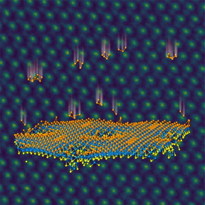 |
| Selenium atoms, represented by orange, implant in a monolayer of blue tungsten and yellow sulfur to form a Janus layer. In the background, electron microscopy confirms atomic positions. CREDIT Oak Ridge National Laboratory, U.S. Dept. of Energy |
Abstract:
A team led by the Department of Energy's Oak Ridge National Laboratory used a simple process to implant atoms precisely into the top layers of ultra-thin crystals, yielding two-sided structures with different chemical compositions. The resulting materials, known as Janus structures after the two-faced Roman god, may prove useful in developing energy and information technologies.
Process for 'two-faced' nanomaterials may aid energy, information tech
Oak Ridge, TN | Posted on June 26th, 2020"We're displacing and replacing only the topmost atoms in a layer that is only three atoms thick, and when we're done, we have a beautiful Janus monolayer where all the atoms in the top are selenium, with tungsten in the middle and sulfur in the bottom," said ORNL's David Geohegan, senior author of the study, which is published in ACS Nano, a journal of the American Chemical Society. "This is the first time that Janus 2D crystals have been fabricated by such a simple process."
Yu-Chuan Lin, a former ORNL postdoctoral fellow who led the study, added, "Janus monolayers are interesting materials because they have a permanent dipole moment in a 2D form, which allows them to separate charge for applications ranging from photovoltaics to quantum information. With this straightforward technique, we can put different atoms on the top or bottom of different layers to explore a variety of other two-faced structures."
This study probed 2D materials called transition metal dichalcogenides, or TMDs, that are valued for their electrical, optical and mechanical properties. Tuning their compositions may improve their abilities to separate charge, catalyze chemical reactions or convert mechanical energy to electrical energy and vice versa.
A single TMD layer is made of a ply of transition metal atoms, such as tungsten or molybdenum, sandwiched between plies of chalcogen atoms, such as sulfur or selenium. A molybdenum disulfide monolayer, for example, features molybdenum atoms between plies of sulfur atoms, structurally similar to a sandwich cookie with a creamy center between two chocolate wafers. Replacing one side's sulfur atoms with selenium atoms produces a Janus monolayer, akin to swapping one of the chocolate wafers with a vanilla one.
Before this study, turning a TMD monolayer into a two-faced structure was more a theoretical feat than an actual experimental accomplishment. In the many scientific papers about Janus monolayers published since 2017, 60 reported theoretical predictions and only two described experiments to synthesize them, according to Lin. This reflects the difficulty in making Janus monolayers due to the significant energy barriers that prevent their growth by typical methods.
In 2015, the ORNL group discovered that pulsed laser deposition could convert molybdenum diselenide to molybdenum disulfide. At the Center for Nanophase Materials Sciences, a DOE Office of Science User Facility at ORNL, pulsed laser deposition is a critical technique for developing quantum materials.
"We speculated that by controlling the kinetic energy of atoms, we could implant them in a monolayer, but we never thought we could achieve such exquisite control," Geohegan said. "Only with atomistic computational modeling and electron microscopy at ORNL were we able to understand how to implant just a fraction of a monolayer, which is amazing."
The method uses a pulsed laser to vaporize a solid target into a hot plasma, which expands from the target toward a substrate. This study used a selenium target to produce a beam-like plasma of clusters of two to nine selenium atoms, which were directed to strike pre-grown tungsten disulfide monolayer crystals.
The key to success in creating two-faced monolayers is bombarding the crystals with a precise amount of energy. Throw a bullet at a door, for example, and it bounces off the surface. But shoot the door and the bullet rips right through. Implanting selenium clusters into only the top of the monolayer is like shooting a door and having the bullet stop in its surface.
"It's not easy to tune your bullets," Geohegan said. The fastest selenium clusters, with energies of 42 electron volts (eV) per atom, ripped through the monolayer; they needed to be controllably slowed to implant into the top ply.
"What's new from this paper is we are using such low energies," said Lin. "People never explored the regime below 10 eV per atom because commercial ion sources only go down to 50 eV at best and don't allow you to choose the atoms you would like to use. However, pulsed laser deposition lets us choose the atoms and explore this energy range fairly easily."
The key to tuning the kinetic energy, Lin said, is to controllably slow the selenium clusters by adding argon gas in a pressure-controlled chamber. Limiting the kinetic energy restricts the penetration of atomically thin layers to specific depths. Injecting a pulse of atom clusters at low energy temporarily crowds and displaces atoms in a region, causing local defects and disorder in the crystal lattice. "The crystal then ejects the extra atoms to heal itself and recrystallizes into an orderly lattice," Geohegan explained. Repeating this implantation and healing process over and over can increase the selenium fraction in the top layer to 100% to complete the formation of a high-quality Janus monolayer.
Controllably implanting and recrystallizing 2D materials in this low-kinetic-energy regime is a new road to making 2D quantum materials. "Janus structures can be made in mere minutes at the low temperatures that are required for semiconductor electronic integration," Lin said, paving the way for production-line manufacturing. Next the researchers want to try making Janus monolayers on flexible substrates useful in mass production, such as plastics.
To prove that they had achieved a Janus structure, Chenze Liu and Gerd Duscher, both of the University of Tennessee, Knoxville, and Matthew Chisholm of ORNL used high-resolution electron microscopy to examine a tilted crystal to identify which atoms were in the top layer (selenium) versus the bottom layer (sulfur).
However, understanding how the process replaced sulfur atoms with larger selenium atoms -- an energetically difficult feat -- was a challenge. ORNL's Mina Yoon used supercomputers at the Oak Ridge Leadership Computing Facility, a DOE Office of Science user facility at ORNL, to calculate the energy dynamics of this uphill battle from theory using first principles.
Further, the scientists needed to understand how energy transferred from clusters to lattices to create local defects. With molecular dynamics simulations, ORNL's Eva Zarkadoula showed clusters of selenium atoms collide with the monolayer at different energies and either bounce off it, crash through it or implant in it -- consistent with the experimental results.
To further confirm the Janus structure, ORNL researchers proved structures had predicted characteristics by calculating their vibrational modes and conducting Raman spectroscopy and X-ray photoelectron spectroscopy experiments.
To understand that the plume was made of clusters, scientists used a combination of optical spectroscopy and mass spectrometry to measure molecular masses and velocities. Taken together, theory and experiment indicated 3 to 5 eV per atom was the optimal energy for precise implantation to form Janus structures.
####
About Oak Ridge National Laboratory
The DOE Office of Science supported the synthesis science, electron microscopy, and computational studies. This research was conducted as a user project at the Center for Nanophase Materials Sciences and used resources of the Oak Ridge Leadership Computing Facility; both are DOE Office of Science User Facilities at ORNL.
UT-Battelle manages ORNL for DOE's Office of Science. The single largest supporter of basic research in the physical sciences in the United States, the Office of Science is working to address some of the most pressing challenges of our time. For more information, please visit https://www.energy.gov/science.
For more information, please click here
Contacts:
Dawn Levy
865-202-9465
@ORNL
Copyright © Oak Ridge National Laboratory
If you have a comment, please Contact us.Issuers of news releases, not 7th Wave, Inc. or Nanotechnology Now, are solely responsible for the accuracy of the content.
Bookmark:


| Related Links |
| Related News Press |
News and information
![]() Quantum computer improves AI predictions April 17th, 2026
Quantum computer improves AI predictions April 17th, 2026
![]() Flexible sensor gains sensitivity under pressure April 17th, 2026
Flexible sensor gains sensitivity under pressure April 17th, 2026
![]() A reusable chip for particulate matter sensing April 17th, 2026
A reusable chip for particulate matter sensing April 17th, 2026
![]() Detecting vibrational quantum beating in the predissociation dynamics of SF6 using time-resolved photoelectron spectroscopy April 17th, 2026
Detecting vibrational quantum beating in the predissociation dynamics of SF6 using time-resolved photoelectron spectroscopy April 17th, 2026
Quantum Physics
![]() Detecting vibrational quantum beating in the predissociation dynamics of SF6 using time-resolved photoelectron spectroscopy April 17th, 2026
Detecting vibrational quantum beating in the predissociation dynamics of SF6 using time-resolved photoelectron spectroscopy April 17th, 2026
![]() Beyond silicon: Electronics at the scale of a single molecule January 30th, 2026
Beyond silicon: Electronics at the scale of a single molecule January 30th, 2026
![]() ICFO researchers overcome long-standing bottleneck in single photon detection with twisted 2D materials August 8th, 2025
ICFO researchers overcome long-standing bottleneck in single photon detection with twisted 2D materials August 8th, 2025
Laboratories
![]() Researchers develop molecular qubits that communicate at telecom frequencies October 3rd, 2025
Researchers develop molecular qubits that communicate at telecom frequencies October 3rd, 2025
Govt.-Legislation/Regulation/Funding/Policy
![]() Quantum computer improves AI predictions April 17th, 2026
Quantum computer improves AI predictions April 17th, 2026
![]() Metasurfaces smooth light to boost magnetic sensing precision January 30th, 2026
Metasurfaces smooth light to boost magnetic sensing precision January 30th, 2026
![]() New imaging approach transforms study of bacterial biofilms August 8th, 2025
New imaging approach transforms study of bacterial biofilms August 8th, 2025
Possible Futures
![]() A fundamentally new therapeutic approach to cystic fibrosis: Nanobody repairs cellular defect April 17th, 2026
A fundamentally new therapeutic approach to cystic fibrosis: Nanobody repairs cellular defect April 17th, 2026
![]() UC Irvine physicists discover method to reverse �quantum scrambling� : The work addresses the problem of information loss in quantum computing system April 17th, 2026
UC Irvine physicists discover method to reverse �quantum scrambling� : The work addresses the problem of information loss in quantum computing system April 17th, 2026
Chip Technology
![]() A reusable chip for particulate matter sensing April 17th, 2026
A reusable chip for particulate matter sensing April 17th, 2026
![]() Metasurfaces smooth light to boost magnetic sensing precision January 30th, 2026
Metasurfaces smooth light to boost magnetic sensing precision January 30th, 2026
Memory Technology
![]() Researchers tackle the memory bottleneck stalling quantum computing October 3rd, 2025
Researchers tackle the memory bottleneck stalling quantum computing October 3rd, 2025
![]() First real-time observation of two-dimensional melting process: Researchers at Mainz University unveil new insights into magnetic vortex structures August 8th, 2025
First real-time observation of two-dimensional melting process: Researchers at Mainz University unveil new insights into magnetic vortex structures August 8th, 2025
![]() Utilizing palladium for addressing contact issues of buried oxide thin film transistors April 5th, 2024
Utilizing palladium for addressing contact issues of buried oxide thin film transistors April 5th, 2024
Discoveries
![]() Quantum computer improves AI predictions April 17th, 2026
Quantum computer improves AI predictions April 17th, 2026
![]() Flexible sensor gains sensitivity under pressure April 17th, 2026
Flexible sensor gains sensitivity under pressure April 17th, 2026
![]() A reusable chip for particulate matter sensing April 17th, 2026
A reusable chip for particulate matter sensing April 17th, 2026
![]() Detecting vibrational quantum beating in the predissociation dynamics of SF6 using time-resolved photoelectron spectroscopy April 17th, 2026
Detecting vibrational quantum beating in the predissociation dynamics of SF6 using time-resolved photoelectron spectroscopy April 17th, 2026
Materials/Metamaterials/Magnetoresistance
![]() First real-time observation of two-dimensional melting process: Researchers at Mainz University unveil new insights into magnetic vortex structures August 8th, 2025
First real-time observation of two-dimensional melting process: Researchers at Mainz University unveil new insights into magnetic vortex structures August 8th, 2025
![]() Researchers unveil a groundbreaking clay-based solution to capture carbon dioxide and combat climate change June 6th, 2025
Researchers unveil a groundbreaking clay-based solution to capture carbon dioxide and combat climate change June 6th, 2025
![]() A 1960s idea inspires NBI researchers to study hitherto inaccessible quantum states June 6th, 2025
A 1960s idea inspires NBI researchers to study hitherto inaccessible quantum states June 6th, 2025
![]() Institute for Nanoscience hosts annual proposal planning meeting May 16th, 2025
Institute for Nanoscience hosts annual proposal planning meeting May 16th, 2025
Announcements
![]() A fundamentally new therapeutic approach to cystic fibrosis: Nanobody repairs cellular defect April 17th, 2026
A fundamentally new therapeutic approach to cystic fibrosis: Nanobody repairs cellular defect April 17th, 2026
![]() UC Irvine physicists discover method to reverse �quantum scrambling� : The work addresses the problem of information loss in quantum computing system April 17th, 2026
UC Irvine physicists discover method to reverse �quantum scrambling� : The work addresses the problem of information loss in quantum computing system April 17th, 2026
Interviews/Book Reviews/Essays/Reports/Podcasts/Journals/White papers/Posters
![]() A fundamentally new therapeutic approach to cystic fibrosis: Nanobody repairs cellular defect April 17th, 2026
A fundamentally new therapeutic approach to cystic fibrosis: Nanobody repairs cellular defect April 17th, 2026
![]() UC Irvine physicists discover method to reverse �quantum scrambling� : The work addresses the problem of information loss in quantum computing system April 17th, 2026
UC Irvine physicists discover method to reverse �quantum scrambling� : The work addresses the problem of information loss in quantum computing system April 17th, 2026
Energy
![]() Sensors innovations for smart lithium-based batteries: advancements, opportunities, and potential challenges August 8th, 2025
Sensors innovations for smart lithium-based batteries: advancements, opportunities, and potential challenges August 8th, 2025
![]() Simple algorithm paired with standard imaging tool could predict failure in lithium metal batteries August 8th, 2025
Simple algorithm paired with standard imaging tool could predict failure in lithium metal batteries August 8th, 2025
Quantum nanoscience
![]() Beyond silicon: Electronics at the scale of a single molecule January 30th, 2026
Beyond silicon: Electronics at the scale of a single molecule January 30th, 2026
![]() MXene nanomaterials enter a new dimension Multilayer nanomaterial: MXene flakes created at Drexel University show new promise as 1D scrolls January 30th, 2026
MXene nanomaterials enter a new dimension Multilayer nanomaterial: MXene flakes created at Drexel University show new promise as 1D scrolls January 30th, 2026
![]() ICFO researchers overcome long-standing bottleneck in single photon detection with twisted 2D materials August 8th, 2025
ICFO researchers overcome long-standing bottleneck in single photon detection with twisted 2D materials August 8th, 2025
|
|
||
|
|
||
| The latest news from around the world, FREE | ||
|
|
||
|
|
||
| Premium Products | ||
|
|
||
|
Only the news you want to read!
Learn More |
||
|
|
||
|
Full-service, expert consulting
Learn More |
||
|
|
||