Home > Press > Heterostructure and Q-factor engineering for low-threshold and persistent nanowire lasing
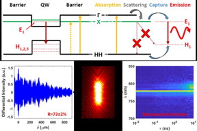 |
| A novel direct-indirect heterostructures is designed, where lasing emission only occurs from quantum well regions but carriers are injected from indirect regions, where recombination is suppressed. This provides a continuous 'topping-up' of carrier density in the quantum well, causing nanosecond lasing after sub-picosecond excitation. Coupled with a mm-scale optical correlation length, corresponding to an end-facet reflectivity of over 70%, these two features provide record-low room-temperature lasing thresholds for near-infrared silicon-integratable nanowire lasers CREDIT by Stefan Skalsky, Yunyan Zhang, Juan Arturo Alanis, H. Aruni Fonseka, Ana M. Sanchez, Huiyun Liu and Patrick Parkinson |
Abstract:
Over the past decade, the idea of photonic computing - where electrons are replaced with light in microelectronic circuits - has emerged as a future technology. This promises low-cost, ultra-high-speed and potentially quantum-enhanced computing, with specific applications in high-efficiency machine learning and neuromorphic computing. While the computing elements and detectors have been developed, the need for nanoscale, high-density and easily-integrated light sources remains unmet. Semiconductor nanowires are seen as a potential candidate, due to their small size (on the order of the wavelength of light), the possibility for direct growth onto industry-standard silicon, and their use of established materials. However, to date, such nanowire lasers on silicon have not been demonstrated to operate continuously at room temperature.
Heterostructure and Q-factor engineering for low-threshold and persistent nanowire lasing
Changchun, China | Posted on March 22nd, 2020In a new paper published in Light Science & Application, scientists from the Photon Science Institute in Manchester, UK with colleagues at University College London and the University of Warwick demonstrate a new route to achieving low-threshold silicon-integratable nanowire lasers. Based on a novel direct-indirect semiconductor heterostructures enabled by the nanowire platform, they demonstrate multi-nanosecond lasing at room temperature. A key design element is the need for high-reflectivity nanowire ends; this is typically a challenging requirement, as common growth methods do not allow simple optimization for high quality end-facets. However, in this study, by employing a novel time-gated interferometer the researchers demonstrate that the reflectivity can be over 70% - around double that expected for a conventional flat-ended laser due to the confinement of light.
Together, the novel material structure and high quality cavity contribute to a low lasing threshold - a measure of the power required to activate lasing in the nanowires - of just 6uJ/cm^2, orders of magnitude lower than previously demonstrated. Not only does this new approach provide high quality nanolasers, but the MBE growth provides a high-yield of functioning wires, with over 85% of nanowires tested working at full power without thermal damage. This high yield is critical for industrial integration of this new structure.
####
For more information, please click here
Contacts:
Patrick Parkinson
Copyright © Changchun Institute of Optics, Fine Mechanics and Physics, Chinese Academy of Sciences
If you have a comment, please Contact us.Issuers of news releases, not 7th Wave, Inc. or Nanotechnology Now, are solely responsible for the accuracy of the content.
Bookmark:


| Related Links |
| Related News Press |
News and information
![]() Quantum computer improves AI predictions April 17th, 2026
Quantum computer improves AI predictions April 17th, 2026
![]() Flexible sensor gains sensitivity under pressure April 17th, 2026
Flexible sensor gains sensitivity under pressure April 17th, 2026
![]() A reusable chip for particulate matter sensing April 17th, 2026
A reusable chip for particulate matter sensing April 17th, 2026
![]() Detecting vibrational quantum beating in the predissociation dynamics of SF6 using time-resolved photoelectron spectroscopy April 17th, 2026
Detecting vibrational quantum beating in the predissociation dynamics of SF6 using time-resolved photoelectron spectroscopy April 17th, 2026
Govt.-Legislation/Regulation/Funding/Policy
![]() Quantum computer improves AI predictions April 17th, 2026
Quantum computer improves AI predictions April 17th, 2026
![]() Metasurfaces smooth light to boost magnetic sensing precision January 30th, 2026
Metasurfaces smooth light to boost magnetic sensing precision January 30th, 2026
![]() New imaging approach transforms study of bacterial biofilms August 8th, 2025
New imaging approach transforms study of bacterial biofilms August 8th, 2025
Possible Futures
![]() A fundamentally new therapeutic approach to cystic fibrosis: Nanobody repairs cellular defect April 17th, 2026
A fundamentally new therapeutic approach to cystic fibrosis: Nanobody repairs cellular defect April 17th, 2026
![]() UC Irvine physicists discover method to reverse �quantum scrambling� : The work addresses the problem of information loss in quantum computing system April 17th, 2026
UC Irvine physicists discover method to reverse �quantum scrambling� : The work addresses the problem of information loss in quantum computing system April 17th, 2026
Chip Technology
![]() A reusable chip for particulate matter sensing April 17th, 2026
A reusable chip for particulate matter sensing April 17th, 2026
![]() Metasurfaces smooth light to boost magnetic sensing precision January 30th, 2026
Metasurfaces smooth light to boost magnetic sensing precision January 30th, 2026
Optical computing/Photonic computing
![]() ICFO researchers overcome long-standing bottleneck in single photon detection with twisted 2D materials August 8th, 2025
ICFO researchers overcome long-standing bottleneck in single photon detection with twisted 2D materials August 8th, 2025
![]() Programmable electron-induced color router array May 14th, 2025
Programmable electron-induced color router array May 14th, 2025
Discoveries
![]() Quantum computer improves AI predictions April 17th, 2026
Quantum computer improves AI predictions April 17th, 2026
![]() Flexible sensor gains sensitivity under pressure April 17th, 2026
Flexible sensor gains sensitivity under pressure April 17th, 2026
![]() A reusable chip for particulate matter sensing April 17th, 2026
A reusable chip for particulate matter sensing April 17th, 2026
![]() Detecting vibrational quantum beating in the predissociation dynamics of SF6 using time-resolved photoelectron spectroscopy April 17th, 2026
Detecting vibrational quantum beating in the predissociation dynamics of SF6 using time-resolved photoelectron spectroscopy April 17th, 2026
Announcements
![]() A fundamentally new therapeutic approach to cystic fibrosis: Nanobody repairs cellular defect April 17th, 2026
A fundamentally new therapeutic approach to cystic fibrosis: Nanobody repairs cellular defect April 17th, 2026
![]() UC Irvine physicists discover method to reverse �quantum scrambling� : The work addresses the problem of information loss in quantum computing system April 17th, 2026
UC Irvine physicists discover method to reverse �quantum scrambling� : The work addresses the problem of information loss in quantum computing system April 17th, 2026
Interviews/Book Reviews/Essays/Reports/Podcasts/Journals/White papers/Posters
![]() A fundamentally new therapeutic approach to cystic fibrosis: Nanobody repairs cellular defect April 17th, 2026
A fundamentally new therapeutic approach to cystic fibrosis: Nanobody repairs cellular defect April 17th, 2026
![]() UC Irvine physicists discover method to reverse �quantum scrambling� : The work addresses the problem of information loss in quantum computing system April 17th, 2026
UC Irvine physicists discover method to reverse �quantum scrambling� : The work addresses the problem of information loss in quantum computing system April 17th, 2026
Grants/Sponsored Research/Awards/Scholarships/Gifts/Contests/Honors/Records
![]() Quantum computer improves AI predictions April 17th, 2026
Quantum computer improves AI predictions April 17th, 2026
![]() Detecting vibrational quantum beating in the predissociation dynamics of SF6 using time-resolved photoelectron spectroscopy April 17th, 2026
Detecting vibrational quantum beating in the predissociation dynamics of SF6 using time-resolved photoelectron spectroscopy April 17th, 2026
![]() Metasurfaces smooth light to boost magnetic sensing precision January 30th, 2026
Metasurfaces smooth light to boost magnetic sensing precision January 30th, 2026
Photonics/Optics/Lasers
![]() Metasurfaces smooth light to boost magnetic sensing precision January 30th, 2026
Metasurfaces smooth light to boost magnetic sensing precision January 30th, 2026
![]() From sensors to smart systems: the rise of AI-driven photonic noses January 30th, 2026
From sensors to smart systems: the rise of AI-driven photonic noses January 30th, 2026
|
|
||
|
|
||
| The latest news from around the world, FREE | ||
|
|
||
|
|
||
| Premium Products | ||
|
|
||
|
Only the news you want to read!
Learn More |
||
|
|
||
|
Full-service, expert consulting
Learn More |
||
|
|
||