Home > Press > On-chip single-mode CdS nanowire laser
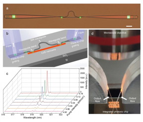 |
| a, optical image of a hybrid MZI structure under excitation. b, the schematic configuration of the on-chip nanowire laser. A CdS nanowire is used as the gain material and is evanescently coupled to an ?-shaped SiN waveguide at both sides to form a hybrid MZI structure. In the coupling area, SiN waveguide bends are predesigned to ensure a high coupling efficiency with excellent reproducibility. Fibre-to-chip grating couplers are designed at both ends of the SiN waveguide, which couple the laser signal from the on-chip SiN waveguide into standard optical fibres for optical characterization. c, Lasing spectra obtained at different pumping intensities above the threshold. The dominant lasing peak is centered at a wavelength of approximately 518.9 nm with a linewidth of approximately 0.1 nm. The side-mode suppression ratio increases with increasing pumping intensity and realizes a maximum value of approximately a factor of 20 (13 dB). d, optical image of the measurement setup under an optical microscope. The measurement setup uses output fibres to collect signals out of the chip via fibre-to-chip grating couplers. CREDIT by Qingyang Bao, Weijia Li, Peizhen Xu, Ming Zhang, Daoxin Dai, Pan Wang, Xin Guo, and Limin Tong |
Abstract:
In the past decade, on-chip nanophotonics has attracted increasing attention for the realization of integrated photonic circuits with faster operation, broader bandwidth, lower power consumption and higher compactness. While a number of on-chip nanophotonic devices and circuits have been successfully fabricated using a complementary metal-oxide semiconductor (CMOS) -compatible technique, on-chip light sources remain challenging. On the other hand, bottom-up grown semiconductor nanowires have long been used for nanoscale waveguide lasers. In recent years, increasing attention has been paid to the integration of active nanowires with on-chip planar waveguides for on-chip light sources. However, due to the large discrepancy in fabrication techniques, refractive index and geometric compatibility between a freestanding nanowire and an on-chip planar waveguide, a variety of issues, including a relatively low coupling efficiency, ineffective mode selection and low reproductivity, have yet to be addressed.
On-chip single-mode CdS nanowire laser
Changchun, China | Posted on March 21st, 2020In a new paper published in Light Science & Application, scientists from the State Key Laboratory of Modern Optical Instrumentation, College of Optical Science and Engineering, Zhejiang University, China demonstrated an on-chip single-mode CdS nanowire laser with high coupling efficiency. The mode selection is realized using a Mach-Zehnder interferometer (MZI) structure. When the pumping intensity exceeds the lasing threshold of 4.9 kW/cm2, on-chip single-mode lasing at approximately 518.9 nm is achieved with a linewidth of 0.1 nm and a side-mode suppression ratio of 20 (13 dB). The output of the nanowire laser is channelled into an on-chip SiN waveguide with high efficiency (up to 58%) by evanescent coupling, and the directional coupling ratio between the two output ports can be varied from 90% to 10% by predesigning the coupling length of the SiN waveguide. Benefitting from the great diversity of the available nanowire materials and high flexibility for bandgap engineering, the on-chip integration scheme demonstrated here can be readily extended to realize on-chip nanolasers from the ultraviolet to near-infrared ranges, which may offer new opportunities for both semiconductor nanowires and on-chip photonic devices.
These scientists summarize the fabrication and operational principle of the laser:
"We use micromanipulation under an optical microscope to integrate a CdS nanowire onto a SiN chip and form a hybrid MZI structure with excellent reproducibility. By using the MZI for mode selection, we operate the laser in single mode. We can also change the output ratios between the two ports of the lasing MZI by using different coupling lengths of the waveguide bends."
"The overall size of the hybrid MZI structure is kept below 100 μm. Fibre-to-chip grating couplers are designed at both ends of the SiN waveguide, which couple the laser signal from the on-chip SiN waveguide into standard optical fibres for optical characterization." "By comparing the lasing output intensities from the nanowire end and the grating area, we estimate the fractional power channelled into the SiN waveguide to be approximately 58%, much higher than previous results obtained in chip integrated nanowire lasers, and can be further improved by optimizing the coupling efficiency between the nanowire and the SiN waveguide." they added.
"Benefitting from the great diversity of the available nanowire materials and high flexibility for bandgap engineering, the on-chip integration scheme demonstrated here can be readily extended to realize on-chip nanolasers from the ultraviolet to near-infrared ranges, and the on-chip single-mode nanowire laser may thus offer an opportunity to develop on-chip physical and biochemical optical sensors with higher stability and compactness. " the scientists forecast.
####
For more information, please click here
Contacts:
Xin Guo
Copyright © Changchun Institute of Optics, Fine Mechanics and Physics, Chinese Academy of Sciences
If you have a comment, please Contact us.Issuers of news releases, not 7th Wave, Inc. or Nanotechnology Now, are solely responsible for the accuracy of the content.
Bookmark:


| Related Links |
| Related News Press |
News and information
![]() Quantum computer improves AI predictions April 17th, 2026
Quantum computer improves AI predictions April 17th, 2026
![]() Flexible sensor gains sensitivity under pressure April 17th, 2026
Flexible sensor gains sensitivity under pressure April 17th, 2026
![]() A reusable chip for particulate matter sensing April 17th, 2026
A reusable chip for particulate matter sensing April 17th, 2026
![]() Detecting vibrational quantum beating in the predissociation dynamics of SF6 using time-resolved photoelectron spectroscopy April 17th, 2026
Detecting vibrational quantum beating in the predissociation dynamics of SF6 using time-resolved photoelectron spectroscopy April 17th, 2026
Govt.-Legislation/Regulation/Funding/Policy
![]() Quantum computer improves AI predictions April 17th, 2026
Quantum computer improves AI predictions April 17th, 2026
![]() Metasurfaces smooth light to boost magnetic sensing precision January 30th, 2026
Metasurfaces smooth light to boost magnetic sensing precision January 30th, 2026
![]() New imaging approach transforms study of bacterial biofilms August 8th, 2025
New imaging approach transforms study of bacterial biofilms August 8th, 2025
Possible Futures
![]() A fundamentally new therapeutic approach to cystic fibrosis: Nanobody repairs cellular defect April 17th, 2026
A fundamentally new therapeutic approach to cystic fibrosis: Nanobody repairs cellular defect April 17th, 2026
![]() UC Irvine physicists discover method to reverse �quantum scrambling� : The work addresses the problem of information loss in quantum computing system April 17th, 2026
UC Irvine physicists discover method to reverse �quantum scrambling� : The work addresses the problem of information loss in quantum computing system April 17th, 2026
Chip Technology
![]() A reusable chip for particulate matter sensing April 17th, 2026
A reusable chip for particulate matter sensing April 17th, 2026
![]() Metasurfaces smooth light to boost magnetic sensing precision January 30th, 2026
Metasurfaces smooth light to boost magnetic sensing precision January 30th, 2026
Sensors
![]() Flexible sensor gains sensitivity under pressure April 17th, 2026
Flexible sensor gains sensitivity under pressure April 17th, 2026
![]() Tiny nanosheets, big leap: A new sensor detects ethanol at ultra-low levels January 30th, 2026
Tiny nanosheets, big leap: A new sensor detects ethanol at ultra-low levels January 30th, 2026
![]() From sensors to smart systems: the rise of AI-driven photonic noses January 30th, 2026
From sensors to smart systems: the rise of AI-driven photonic noses January 30th, 2026
![]() Sensors innovations for smart lithium-based batteries: advancements, opportunities, and potential challenges August 8th, 2025
Sensors innovations for smart lithium-based batteries: advancements, opportunities, and potential challenges August 8th, 2025
Discoveries
![]() Quantum computer improves AI predictions April 17th, 2026
Quantum computer improves AI predictions April 17th, 2026
![]() Flexible sensor gains sensitivity under pressure April 17th, 2026
Flexible sensor gains sensitivity under pressure April 17th, 2026
![]() A reusable chip for particulate matter sensing April 17th, 2026
A reusable chip for particulate matter sensing April 17th, 2026
![]() Detecting vibrational quantum beating in the predissociation dynamics of SF6 using time-resolved photoelectron spectroscopy April 17th, 2026
Detecting vibrational quantum beating in the predissociation dynamics of SF6 using time-resolved photoelectron spectroscopy April 17th, 2026
Announcements
![]() A fundamentally new therapeutic approach to cystic fibrosis: Nanobody repairs cellular defect April 17th, 2026
A fundamentally new therapeutic approach to cystic fibrosis: Nanobody repairs cellular defect April 17th, 2026
![]() UC Irvine physicists discover method to reverse �quantum scrambling� : The work addresses the problem of information loss in quantum computing system April 17th, 2026
UC Irvine physicists discover method to reverse �quantum scrambling� : The work addresses the problem of information loss in quantum computing system April 17th, 2026
Interviews/Book Reviews/Essays/Reports/Podcasts/Journals/White papers/Posters
![]() A fundamentally new therapeutic approach to cystic fibrosis: Nanobody repairs cellular defect April 17th, 2026
A fundamentally new therapeutic approach to cystic fibrosis: Nanobody repairs cellular defect April 17th, 2026
![]() UC Irvine physicists discover method to reverse �quantum scrambling� : The work addresses the problem of information loss in quantum computing system April 17th, 2026
UC Irvine physicists discover method to reverse �quantum scrambling� : The work addresses the problem of information loss in quantum computing system April 17th, 2026
Photonics/Optics/Lasers
![]() Metasurfaces smooth light to boost magnetic sensing precision January 30th, 2026
Metasurfaces smooth light to boost magnetic sensing precision January 30th, 2026
![]() From sensors to smart systems: the rise of AI-driven photonic noses January 30th, 2026
From sensors to smart systems: the rise of AI-driven photonic noses January 30th, 2026
|
|
||
|
|
||
| The latest news from around the world, FREE | ||
|
|
||
|
|
||
| Premium Products | ||
|
|
||
|
Only the news you want to read!
Learn More |
||
|
|
||
|
Full-service, expert consulting
Learn More |
||
|
|
||