Home > Press > Optical vacuum cleaner can manipulate nanoparticles: The TPU and international researchers developed a concept for constructing an optical vacuum cleaner; due to its optical properties, it can trap nanoparticles from the environment; currently, there are no sufficiently effective
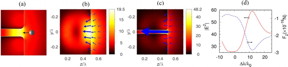 |
| (a) Schematic diagram for the "optical vacuum cleaner", where a nanoparticle is pulled by the optical force, and moves towards the nanohole structured dielectric cuboid. (b,c) Light intensity (|E|2) and optical force distributions for (b) solid cuboid without a hole, (c) cuboid with a 20?nm hole. The refractive index and size of the simulated cuboids are set to be n?=?2 and L?=?λ. (d) Optical force and light intensity vs illumination wavelength, at the opening of the nanohole. The optical force is assumed to be exerted on a gold nanosphere with the radius of d?=?15?nm and complex dielectric permittivity εp?=??9.421?+?1.504 i at λ?=?600?nm35, and calculated using the dipole approximation. The arrows in blue color represent the optical gradient force. CREDIT Tomsk Polytechnic University |
Abstract:
Scientists of Tomsk Polytechnic University jointly with Russian and international colleagues developed the concept for constructing an "optical vacuum cleaner". Due to its optical properties, it can trap nanoparticles from the environment. Currently, there are no effective devices for this task. The research results were published in Scientific Reports (IF:4,525; Q1). In the future, such "vacuum cleaners" can be utilized for air purification during lab-on-a-chip operations and preparation of clean rooms.
Optical vacuum cleaner can manipulate nanoparticles: The TPU and international researchers developed a concept for constructing an optical vacuum cleaner; due to its optical properties, it can trap nanoparticles from the environment; currently, there are no sufficiently effective
Tomsk, Russia | Posted on September 13th, 2019"The size of nanoparticles varies from 1 to a maximum of 100 nanometers. Currently, researchers from all around the world are seeking for the ways to control such small particles and manipulate them for various applications. However, there have been no sufficiently effective and widely used devices for such tasks yet. We offer a new concept for particle manipulation and capture - it is "optical vacuum cleaner" - says Oleg Minin, Professor of the TPU Division for Electronic Engineering.
According to this concept, an "optical vacuum cleaner" is a dielectric microparticle. In the published article, the scientists used particles having the shape of an equilateral cuboid. The particles have a nanoscale gouge or nanohole. When they are exposed to optical radiation, such as laser, there is optical pressure.
"The resultant force is directed inside our cuboid, trapping nanoparticles into the hole. The ?apacity, respectively, depends on the size of the hole", - says the scientist.
This concept can be implemented in the so-called lab-on-a-chip work in biomedical research. This technique can combine several laboratory functions on a chip, varying in size from a few square millimeters to square centimeters. This advanced on-chip analysis method will allow achieving high-throughput screening and automation. Cleaning chip surface and ambient air from foreign nanoparticles will allow increasing the analyzes sensitivity and the result accuracy.
The study was conduct by Russian and international specialists from Jilin University (China) and Ben-Gurion University (Israel). The next stage will be experimental confirmation of the concept.
####
For more information, please click here
Contacts:
Vitalii Sdelnikov
7-382-260-6404
Copyright © Tomsk Polytechnic University
If you have a comment, please Contact us.Issuers of news releases, not 7th Wave, Inc. or Nanotechnology Now, are solely responsible for the accuracy of the content.
Bookmark:


| Related Links |
| Related News Press |
News and information
![]() Quantum computer improves AI predictions April 17th, 2026
Quantum computer improves AI predictions April 17th, 2026
![]() Flexible sensor gains sensitivity under pressure April 17th, 2026
Flexible sensor gains sensitivity under pressure April 17th, 2026
![]() A reusable chip for particulate matter sensing April 17th, 2026
A reusable chip for particulate matter sensing April 17th, 2026
![]() Detecting vibrational quantum beating in the predissociation dynamics of SF6 using time-resolved photoelectron spectroscopy April 17th, 2026
Detecting vibrational quantum beating in the predissociation dynamics of SF6 using time-resolved photoelectron spectroscopy April 17th, 2026
Lab-on-a-chip
![]() Micro-scale opto-thermo-mechanical actuation in the dry adhesive regime Peer-Reviewed Publication September 24th, 2021
Micro-scale opto-thermo-mechanical actuation in the dry adhesive regime Peer-Reviewed Publication September 24th, 2021
![]() Silicon-graphene hybrid plasmonic waveguide photodetectors beyond 1.55 μm March 13th, 2020
Silicon-graphene hybrid plasmonic waveguide photodetectors beyond 1.55 μm March 13th, 2020
Possible Futures
![]() A fundamentally new therapeutic approach to cystic fibrosis: Nanobody repairs cellular defect April 17th, 2026
A fundamentally new therapeutic approach to cystic fibrosis: Nanobody repairs cellular defect April 17th, 2026
![]() UC Irvine physicists discover method to reverse �quantum scrambling� : The work addresses the problem of information loss in quantum computing system April 17th, 2026
UC Irvine physicists discover method to reverse �quantum scrambling� : The work addresses the problem of information loss in quantum computing system April 17th, 2026
Chip Technology
![]() A reusable chip for particulate matter sensing April 17th, 2026
A reusable chip for particulate matter sensing April 17th, 2026
![]() Metasurfaces smooth light to boost magnetic sensing precision January 30th, 2026
Metasurfaces smooth light to boost magnetic sensing precision January 30th, 2026
Nanoelectronics
![]() Lab to industry: InSe wafer-scale breakthrough for future electronics August 8th, 2025
Lab to industry: InSe wafer-scale breakthrough for future electronics August 8th, 2025
![]() Interdisciplinary: Rice team tackles the future of semiconductors Multiferroics could be the key to ultralow-energy computing October 6th, 2023
Interdisciplinary: Rice team tackles the future of semiconductors Multiferroics could be the key to ultralow-energy computing October 6th, 2023
![]() Key element for a scalable quantum computer: Physicists from Forschungszentrum J�lich and RWTH Aachen University demonstrate electron transport on a quantum chip September 23rd, 2022
Key element for a scalable quantum computer: Physicists from Forschungszentrum J�lich and RWTH Aachen University demonstrate electron transport on a quantum chip September 23rd, 2022
![]() Reduced power consumption in semiconductor devices September 23rd, 2022
Reduced power consumption in semiconductor devices September 23rd, 2022
Discoveries
![]() Quantum computer improves AI predictions April 17th, 2026
Quantum computer improves AI predictions April 17th, 2026
![]() Flexible sensor gains sensitivity under pressure April 17th, 2026
Flexible sensor gains sensitivity under pressure April 17th, 2026
![]() A reusable chip for particulate matter sensing April 17th, 2026
A reusable chip for particulate matter sensing April 17th, 2026
![]() Detecting vibrational quantum beating in the predissociation dynamics of SF6 using time-resolved photoelectron spectroscopy April 17th, 2026
Detecting vibrational quantum beating in the predissociation dynamics of SF6 using time-resolved photoelectron spectroscopy April 17th, 2026
Announcements
![]() A fundamentally new therapeutic approach to cystic fibrosis: Nanobody repairs cellular defect April 17th, 2026
A fundamentally new therapeutic approach to cystic fibrosis: Nanobody repairs cellular defect April 17th, 2026
![]() UC Irvine physicists discover method to reverse �quantum scrambling� : The work addresses the problem of information loss in quantum computing system April 17th, 2026
UC Irvine physicists discover method to reverse �quantum scrambling� : The work addresses the problem of information loss in quantum computing system April 17th, 2026
Interviews/Book Reviews/Essays/Reports/Podcasts/Journals/White papers/Posters
![]() A fundamentally new therapeutic approach to cystic fibrosis: Nanobody repairs cellular defect April 17th, 2026
A fundamentally new therapeutic approach to cystic fibrosis: Nanobody repairs cellular defect April 17th, 2026
![]() UC Irvine physicists discover method to reverse �quantum scrambling� : The work addresses the problem of information loss in quantum computing system April 17th, 2026
UC Irvine physicists discover method to reverse �quantum scrambling� : The work addresses the problem of information loss in quantum computing system April 17th, 2026
Tools
![]() Metasurfaces smooth light to boost magnetic sensing precision January 30th, 2026
Metasurfaces smooth light to boost magnetic sensing precision January 30th, 2026
![]() From sensors to smart systems: the rise of AI-driven photonic noses January 30th, 2026
From sensors to smart systems: the rise of AI-driven photonic noses January 30th, 2026
![]() Japan launches fully domestically produced quantum computer: Expo visitors to experience quantum computing firsthand August 8th, 2025
Japan launches fully domestically produced quantum computer: Expo visitors to experience quantum computing firsthand August 8th, 2025
Photonics/Optics/Lasers
![]() Metasurfaces smooth light to boost magnetic sensing precision January 30th, 2026
Metasurfaces smooth light to boost magnetic sensing precision January 30th, 2026
![]() From sensors to smart systems: the rise of AI-driven photonic noses January 30th, 2026
From sensors to smart systems: the rise of AI-driven photonic noses January 30th, 2026
|
|
||
|
|
||
| The latest news from around the world, FREE | ||
|
|
||
|
|
||
| Premium Products | ||
|
|
||
|
Only the news you want to read!
Learn More |
||
|
|
||
|
Full-service, expert consulting
Learn More |
||
|
|
||