Home > Press > NRL, AFRL develop direct-write quantum calligraphy in monolayer semiconductors
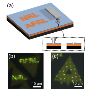 |
| (a) Illustration showing an AFM tip indenting the TMD/polymer structure to introduce local strain. (b) Patterned single photon emission in WSe2 induced by AFM indentation of the letters 'NRL' and 'AFRL'. (c) AFM indents produce single photon emitter 'ornaments' on a monolayer WSe2 'Christmas tree.' CREDIT US Naval Research Laboratory |
Abstract:
Scientists at the U.S. Naval Research Laboratory (NRL) and the Air Force Research Laboratory (AFRL) have developed a way to directly write quantum light sources, which emit a single photon of light at a time, into monolayer semiconductors such as tungsten diselenide (WSe2). Single photon emitters (SPEs), or quantum emitters, are key components in a wide range of nascent quantum-based technologies, including computing, secure communications, sensing and metrology.
NRL, AFRL develop direct-write quantum calligraphy in monolayer semiconductors
Washington, DC | Posted on February 15th, 2019
In contrast with conventional light emitting diodes which emit billions of photons simultaneously to form a steady stream of light, an ideal SPE generates exactly one photon on demand, with each photon indistinguishable from another. These characteristics are essential for photon-based quantum technologies under development. In addition, such capabilities should be realized in a material platform which enables precise, repeatable placement of SPEs in a fully scalable fashion compatible with existing semiconductor chip manufacturing.
NRL scientists used an atomic force microscope (AFM) to create nanoscale depressions or indents in a single monolayer of WSe2 on a polymer film substrate. A highly localized strain field is produced around the nano-indent which creates the single photon emitter state in the WSe2. Time correlated measurements performed at AFRL of this light emission confirmed the true single photon nature of these states. These emitters are bright, producing high rates of single photons, and spectrally stable, key requirements for emerging applications.
"This quantum calligraphy allows deterministic placement and real time design of arbitrary patterns of SPEs for facile coupling with photonic waveguides, cavities and plasmonic structures," said Berend Jonker, Ph.D., senior scientist and principal investigator. "Our results also indicate that a nano-imprinting approach will be effective in creating large arrays or patterns of quantum emitters for wafer scale manufacturing of quantum photonic systems."
Dr. Matthew Rosenberger, lead author of the study, points out the importance of this discovery stating, "In addition to enabling versatile placement of SPEs, these results present a general methodology for imparting strain into two dimensional (2D) materials with nanometer-scale precision, providing an invaluable tool for further investigations and future applications of strain engineering of 2D devices."
The results of this study pave the way for the use of 2D materials as solid state hosts for single photon emitters in applications relevant to the Department of Defense (DoD) mission, such as secure communications, sensing and quantum computation. Such applications enable communication between distant DoD forces which is not vulnerable to eavesdropping or decryption, an essential requirement to insure the safety of the warfighter.
Quantum computation on a chip provides onboard capability to rapidly analyze very large data sets acquired by sensor arrays, so that the entire data set does not have to be transmitted, reducing bandwidth requirements. The research results are reported in the January 2019 ACS Nano (DOI: 10.1021/acsnano.8b08730).
The research team included Dr. Matthew Rosenberger, Dr. Hsun-Jen Chuang, Dr. Saujan Sivaram, Dr. Kathleen McCreary, and Dr. Berend Jonker from the NRL Materials Science and Technology Division; and Dr. Chandriker Kavir Dass and Dr. Joshua R. Hendrickson from the AFRL Sensors Directorate. Both Rosenberger and Sivaram hold National Research Council (NRC) fellowships at NRL, and Chuang holds an American Society for Engineering Education (ASEE) fellowship at NRL.
####
For more information, please click here
Contacts:
Daniel Parry
202-767-2326
Copyright © Naval Research Laboratory
If you have a comment, please Contact us.Issuers of news releases, not 7th Wave, Inc. or Nanotechnology Now, are solely responsible for the accuracy of the content.
Bookmark:


| Related Links |
| Related News Press |
News and information
![]() Quantum computer improves AI predictions April 17th, 2026
Quantum computer improves AI predictions April 17th, 2026
![]() Flexible sensor gains sensitivity under pressure April 17th, 2026
Flexible sensor gains sensitivity under pressure April 17th, 2026
![]() A reusable chip for particulate matter sensing April 17th, 2026
A reusable chip for particulate matter sensing April 17th, 2026
![]() Detecting vibrational quantum beating in the predissociation dynamics of SF6 using time-resolved photoelectron spectroscopy April 17th, 2026
Detecting vibrational quantum beating in the predissociation dynamics of SF6 using time-resolved photoelectron spectroscopy April 17th, 2026
Govt.-Legislation/Regulation/Funding/Policy
![]() Quantum computer improves AI predictions April 17th, 2026
Quantum computer improves AI predictions April 17th, 2026
![]() Metasurfaces smooth light to boost magnetic sensing precision January 30th, 2026
Metasurfaces smooth light to boost magnetic sensing precision January 30th, 2026
![]() New imaging approach transforms study of bacterial biofilms August 8th, 2025
New imaging approach transforms study of bacterial biofilms August 8th, 2025
Possible Futures
![]() A fundamentally new therapeutic approach to cystic fibrosis: Nanobody repairs cellular defect April 17th, 2026
A fundamentally new therapeutic approach to cystic fibrosis: Nanobody repairs cellular defect April 17th, 2026
![]() UC Irvine physicists discover method to reverse �quantum scrambling� : The work addresses the problem of information loss in quantum computing system April 17th, 2026
UC Irvine physicists discover method to reverse �quantum scrambling� : The work addresses the problem of information loss in quantum computing system April 17th, 2026
Chip Technology
![]() A reusable chip for particulate matter sensing April 17th, 2026
A reusable chip for particulate matter sensing April 17th, 2026
![]() Metasurfaces smooth light to boost magnetic sensing precision January 30th, 2026
Metasurfaces smooth light to boost magnetic sensing precision January 30th, 2026
Optical computing/Photonic computing
![]() ICFO researchers overcome long-standing bottleneck in single photon detection with twisted 2D materials August 8th, 2025
ICFO researchers overcome long-standing bottleneck in single photon detection with twisted 2D materials August 8th, 2025
![]() Programmable electron-induced color router array May 14th, 2025
Programmable electron-induced color router array May 14th, 2025
Sensors
![]() Flexible sensor gains sensitivity under pressure April 17th, 2026
Flexible sensor gains sensitivity under pressure April 17th, 2026
![]() Tiny nanosheets, big leap: A new sensor detects ethanol at ultra-low levels January 30th, 2026
Tiny nanosheets, big leap: A new sensor detects ethanol at ultra-low levels January 30th, 2026
![]() From sensors to smart systems: the rise of AI-driven photonic noses January 30th, 2026
From sensors to smart systems: the rise of AI-driven photonic noses January 30th, 2026
![]() Sensors innovations for smart lithium-based batteries: advancements, opportunities, and potential challenges August 8th, 2025
Sensors innovations for smart lithium-based batteries: advancements, opportunities, and potential challenges August 8th, 2025
Discoveries
![]() Quantum computer improves AI predictions April 17th, 2026
Quantum computer improves AI predictions April 17th, 2026
![]() Flexible sensor gains sensitivity under pressure April 17th, 2026
Flexible sensor gains sensitivity under pressure April 17th, 2026
![]() A reusable chip for particulate matter sensing April 17th, 2026
A reusable chip for particulate matter sensing April 17th, 2026
![]() Detecting vibrational quantum beating in the predissociation dynamics of SF6 using time-resolved photoelectron spectroscopy April 17th, 2026
Detecting vibrational quantum beating in the predissociation dynamics of SF6 using time-resolved photoelectron spectroscopy April 17th, 2026
Announcements
![]() A fundamentally new therapeutic approach to cystic fibrosis: Nanobody repairs cellular defect April 17th, 2026
A fundamentally new therapeutic approach to cystic fibrosis: Nanobody repairs cellular defect April 17th, 2026
![]() UC Irvine physicists discover method to reverse �quantum scrambling� : The work addresses the problem of information loss in quantum computing system April 17th, 2026
UC Irvine physicists discover method to reverse �quantum scrambling� : The work addresses the problem of information loss in quantum computing system April 17th, 2026
Interviews/Book Reviews/Essays/Reports/Podcasts/Journals/White papers/Posters
![]() A fundamentally new therapeutic approach to cystic fibrosis: Nanobody repairs cellular defect April 17th, 2026
A fundamentally new therapeutic approach to cystic fibrosis: Nanobody repairs cellular defect April 17th, 2026
![]() UC Irvine physicists discover method to reverse �quantum scrambling� : The work addresses the problem of information loss in quantum computing system April 17th, 2026
UC Irvine physicists discover method to reverse �quantum scrambling� : The work addresses the problem of information loss in quantum computing system April 17th, 2026
Military
![]() Quantum engineers �squeeze� laser frequency combs to make more sensitive gas sensors January 17th, 2025
Quantum engineers �squeeze� laser frequency combs to make more sensitive gas sensors January 17th, 2025
![]() Chainmail-like material could be the future of armor: First 2D mechanically interlocked polymer exhibits exceptional flexibility and strength January 17th, 2025
Chainmail-like material could be the future of armor: First 2D mechanically interlocked polymer exhibits exceptional flexibility and strength January 17th, 2025
![]() Single atoms show their true color July 5th, 2024
Single atoms show their true color July 5th, 2024
![]() NRL charters Navy�s quantum inertial navigation path to reduce drift April 5th, 2024
NRL charters Navy�s quantum inertial navigation path to reduce drift April 5th, 2024
Photonics/Optics/Lasers
![]() Metasurfaces smooth light to boost magnetic sensing precision January 30th, 2026
Metasurfaces smooth light to boost magnetic sensing precision January 30th, 2026
![]() From sensors to smart systems: the rise of AI-driven photonic noses January 30th, 2026
From sensors to smart systems: the rise of AI-driven photonic noses January 30th, 2026
Quantum nanoscience
![]() Beyond silicon: Electronics at the scale of a single molecule January 30th, 2026
Beyond silicon: Electronics at the scale of a single molecule January 30th, 2026
![]() MXene nanomaterials enter a new dimension Multilayer nanomaterial: MXene flakes created at Drexel University show new promise as 1D scrolls January 30th, 2026
MXene nanomaterials enter a new dimension Multilayer nanomaterial: MXene flakes created at Drexel University show new promise as 1D scrolls January 30th, 2026
![]() ICFO researchers overcome long-standing bottleneck in single photon detection with twisted 2D materials August 8th, 2025
ICFO researchers overcome long-standing bottleneck in single photon detection with twisted 2D materials August 8th, 2025
|
|
||
|
|
||
| The latest news from around the world, FREE | ||
|
|
||
|
|
||
| Premium Products | ||
|
|
||
|
Only the news you want to read!
Learn More |
||
|
|
||
|
Full-service, expert consulting
Learn More |
||
|
|
||