Home > Press > Large, stable pieces of graphene produced with unique edge pattern: Breakthrough in graphene research
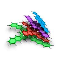 |
| The much sought-after zigzag pattern can be found either in staggered rows of honeycombs (blue and purple) or four-limbed stars surrounding a central point of four graphene honeycombs (red and green). (Image: FAU/Konstantin Amsharov) |
Abstract:
Graphene is a promising material for use in nanoelectronics. Its electronic properties depend greatly, however, on how the edges of the carbon layer are formed. Zigzag patterns are particularly interesting in this respect, but until now it has been virtually impossible to create edges with a pattern like this. Chemists and physicists at FAU have now succeeded in producing stable nanographene with a zigzag edge. Not only that, the method they used was even comparatively simple. Their research, conducted within the framework of collaborative research centre 953 - Synthetic Carbon Allotropes funded by the German Research Foundation (DFG), has now been published in the journal Nature Communications.
Large, stable pieces of graphene produced with unique edge pattern: Breakthrough in graphene research
Erlangen, Germany | Posted on February 1st, 2019Bay, fjord, cove, armchair and zigzag - when chemists use terms such as these, it is clear that they are referring to nanographene. More specifically, the shape taken by the edges of nanographene, i.e. small fragments of graphene. Graphene consists of a single-layered carbon structure, where each carbon atom is surrounded by three others. This creates a pattern reminiscent of a honeycomb, with atoms in each of the corners. Nanographene is a promising candidate for use in the field of microelectronics, taking over from silicon which is used today and bringing microelectronics down to the nano scale.
The electronic properties of the material depend greatly on its shape, size and above all, periphery, in other words how the edges are structured. A zigzag periphery is particularly suitable, as in this case the electrons, which act as charge carriers, are more mobile than in other edge structures. This means that using pieces of zigzag-shaped graphene in nanoelectronic components may allow higher frequencies for switches.
The problem currently faced by materials scientists who want to research only zigzag nanographene is that this form makes the compounds rather unstable, and unable to be produced in a controlled manner. This is a prerequisite, however, if the electronic properties are to be investigated in detail.
The team of researchers led by PD Dr. Konstantin Amsharov from the Chair of Organic Chemistry II have now succeeded in doing just that. Not only have they discovered a straightforward method for synthesising zigzag nanographene, their procedure delivers a yield of close to one hundred percent and is suitable for large scale production. They have already produced a technically relevant quantity in the laboratory.
First of all, the FAU researchers produce preliminary molecules, which they then fitt together in a honeycomb formation over several cycles, in a process known as cyclisation. In the end, graphene fragments are produced from staggered rows of honeycombs or four-limbed stars surrounding a central point of four graphene honeycombs, with the sought-after zigzag pattern to their edges. Why is this method able to produce stable zigzag nanographene? The explanation lies in the fact that the product crystallises directly even during synthesis. In their solid state, the molecules are not in contact with oxygen. In solution, however, oxidation causes the structures to disintegrate quickly.
This approach allows scientists to produce large pieces of graphene, whilst maintaining control over their shape and periphery. This breakthrough in graphene research means that scientists should soon be able to produce and research a variety of interesting nanographene structures, a crucial step towards finally being able to use the material in nanoelectronic components.
####
For more information, please click here
Contacts:
FAU Press Office
49-913-185-70229
Copyright © UNIVERSITY OF ERLANGEN-NUREMBERG
If you have a comment, please Contact us.Issuers of news releases, not 7th Wave, Inc. or Nanotechnology Now, are solely responsible for the accuracy of the content.
Bookmark:


| Related Links |
| Related News Press |
News and information
![]() Quantum computer improves AI predictions April 17th, 2026
Quantum computer improves AI predictions April 17th, 2026
![]() Flexible sensor gains sensitivity under pressure April 17th, 2026
Flexible sensor gains sensitivity under pressure April 17th, 2026
![]() A reusable chip for particulate matter sensing April 17th, 2026
A reusable chip for particulate matter sensing April 17th, 2026
![]() Detecting vibrational quantum beating in the predissociation dynamics of SF6 using time-resolved photoelectron spectroscopy April 17th, 2026
Detecting vibrational quantum beating in the predissociation dynamics of SF6 using time-resolved photoelectron spectroscopy April 17th, 2026
2 Dimensional Materials
![]() Flexible sensor gains sensitivity under pressure April 17th, 2026
Flexible sensor gains sensitivity under pressure April 17th, 2026
Graphene/ Graphite
![]() Electrifying results shed light on graphene foam as a potential material for lab grown cartilage June 6th, 2025
Electrifying results shed light on graphene foam as a potential material for lab grown cartilage June 6th, 2025
![]() Breakthrough in proton barrier films using pore-free graphene oxide: Kumamoto University researchers achieve new milestone in advanced coating technologies September 13th, 2024
Breakthrough in proton barrier films using pore-free graphene oxide: Kumamoto University researchers achieve new milestone in advanced coating technologies September 13th, 2024
Possible Futures
![]() A fundamentally new therapeutic approach to cystic fibrosis: Nanobody repairs cellular defect April 17th, 2026
A fundamentally new therapeutic approach to cystic fibrosis: Nanobody repairs cellular defect April 17th, 2026
![]() UC Irvine physicists discover method to reverse �quantum scrambling� : The work addresses the problem of information loss in quantum computing system April 17th, 2026
UC Irvine physicists discover method to reverse �quantum scrambling� : The work addresses the problem of information loss in quantum computing system April 17th, 2026
Chip Technology
![]() A reusable chip for particulate matter sensing April 17th, 2026
A reusable chip for particulate matter sensing April 17th, 2026
![]() Metasurfaces smooth light to boost magnetic sensing precision January 30th, 2026
Metasurfaces smooth light to boost magnetic sensing precision January 30th, 2026
Nanoelectronics
![]() Lab to industry: InSe wafer-scale breakthrough for future electronics August 8th, 2025
Lab to industry: InSe wafer-scale breakthrough for future electronics August 8th, 2025
![]() Interdisciplinary: Rice team tackles the future of semiconductors Multiferroics could be the key to ultralow-energy computing October 6th, 2023
Interdisciplinary: Rice team tackles the future of semiconductors Multiferroics could be the key to ultralow-energy computing October 6th, 2023
![]() Key element for a scalable quantum computer: Physicists from Forschungszentrum J�lich and RWTH Aachen University demonstrate electron transport on a quantum chip September 23rd, 2022
Key element for a scalable quantum computer: Physicists from Forschungszentrum J�lich and RWTH Aachen University demonstrate electron transport on a quantum chip September 23rd, 2022
![]() Reduced power consumption in semiconductor devices September 23rd, 2022
Reduced power consumption in semiconductor devices September 23rd, 2022
Discoveries
![]() Quantum computer improves AI predictions April 17th, 2026
Quantum computer improves AI predictions April 17th, 2026
![]() Flexible sensor gains sensitivity under pressure April 17th, 2026
Flexible sensor gains sensitivity under pressure April 17th, 2026
![]() A reusable chip for particulate matter sensing April 17th, 2026
A reusable chip for particulate matter sensing April 17th, 2026
![]() Detecting vibrational quantum beating in the predissociation dynamics of SF6 using time-resolved photoelectron spectroscopy April 17th, 2026
Detecting vibrational quantum beating in the predissociation dynamics of SF6 using time-resolved photoelectron spectroscopy April 17th, 2026
Materials/Metamaterials/Magnetoresistance
![]() First real-time observation of two-dimensional melting process: Researchers at Mainz University unveil new insights into magnetic vortex structures August 8th, 2025
First real-time observation of two-dimensional melting process: Researchers at Mainz University unveil new insights into magnetic vortex structures August 8th, 2025
![]() Researchers unveil a groundbreaking clay-based solution to capture carbon dioxide and combat climate change June 6th, 2025
Researchers unveil a groundbreaking clay-based solution to capture carbon dioxide and combat climate change June 6th, 2025
![]() A 1960s idea inspires NBI researchers to study hitherto inaccessible quantum states June 6th, 2025
A 1960s idea inspires NBI researchers to study hitherto inaccessible quantum states June 6th, 2025
![]() Institute for Nanoscience hosts annual proposal planning meeting May 16th, 2025
Institute for Nanoscience hosts annual proposal planning meeting May 16th, 2025
Announcements
![]() A fundamentally new therapeutic approach to cystic fibrosis: Nanobody repairs cellular defect April 17th, 2026
A fundamentally new therapeutic approach to cystic fibrosis: Nanobody repairs cellular defect April 17th, 2026
![]() UC Irvine physicists discover method to reverse �quantum scrambling� : The work addresses the problem of information loss in quantum computing system April 17th, 2026
UC Irvine physicists discover method to reverse �quantum scrambling� : The work addresses the problem of information loss in quantum computing system April 17th, 2026
Interviews/Book Reviews/Essays/Reports/Podcasts/Journals/White papers/Posters
![]() A fundamentally new therapeutic approach to cystic fibrosis: Nanobody repairs cellular defect April 17th, 2026
A fundamentally new therapeutic approach to cystic fibrosis: Nanobody repairs cellular defect April 17th, 2026
![]() UC Irvine physicists discover method to reverse �quantum scrambling� : The work addresses the problem of information loss in quantum computing system April 17th, 2026
UC Irvine physicists discover method to reverse �quantum scrambling� : The work addresses the problem of information loss in quantum computing system April 17th, 2026
|
|
||
|
|
||
| The latest news from around the world, FREE | ||
|
|
||
|
|
||
| Premium Products | ||
|
|
||
|
Only the news you want to read!
Learn More |
||
|
|
||
|
Full-service, expert consulting
Learn More |
||
|
|
||