Home > Press > Scientists use magnetic defects to achieve electromagnetic wave breakthrough
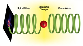 |
| This shows how a plane electron wave and a magnetic charge interact, forming an electron vortex state that carries orbital angular momentum. CREDIT Argonne National Laboratory |
Abstract:
Surfers spend much of their time watching long waves come onto the shoreline as they attempt to catch one right as it begins to curve and break.
Scientists use magnetic defects to achieve electromagnetic wave breakthrough
Argonne, IL | Posted on December 20th, 2018In a similar vein, scientists are working to create twisting helical electromagnetic waves whose curvature allows more accurate imaging of the magnetic properties of different materials at the atomic level and could possibly lead to the development of future devices.
When scientists use electron beams to look at samples of materials, they have the ability to modify many different aspects of the electromagnetic waves that make up the beam. They can make the amplitude of the waves bigger or smaller, or make the waves faster or slower. However, until now there has been no easy way to transform a plane wave -- like the long rolling waves out at sea -- into a helical wave, like the ones that crash on shore.
"If we can see the magnetic moments of the material, we can build a description of the total magnetic properties of the material, and how the material will manifest its electronic and magnetic properties." -- C.D. Phatak, Argonne materials scientist
In a new study from the U.S. Department of Energy's (DOE) Argonne National Laboratory, scientists have created small regions of magnetic defects made from nanoscale magnetic islands assembled into a grid. The plane waves interact with these defects, thereby generating helical waves.
"We're looking for waves with a kind of perfect curl, and in order to generate the curl we need to give them something to crash into, which in our case are magnetic monopoles," said Argonne materials scientist Charudatta (C.D.) Phatak.
The reason scientists are so interested in helical waves is that they have a property called orbital angular momentum. Knowing the orbital angular momentum of an electron beam allows scientists to investigate the magnetic behavior of materials at an atomic level by determining an atomic property called the magnetic moment.
"If we can see the magnetic moments of the material, we can build a description of the total magnetic properties of the material, and how the material will manifest its electronic and magnetic properties," Phatak said.
In this way, the refigured electron beam could be useful for studying materials in which spin and magnetization play a crucial role, potentially paving the way towards new forms of electronic devices.
Having access to the information encoded by orbital angular momentum will also allow scientists to better understand the nuances of chiral materials, which have a kind of left- or right-handedness that determines their properties.
The grid of defects can be inserted into any transmission electron microscope to provide a direct way of imaging the sample. "People usually don't think about modifying the beam profile itself in this way," Phatak said.
In the next phase of the experiment, Phatak explained that the researchers may seek to replace the grids of magnetic islands with solenoids, or coils of wire that can act as electromagnets. Using solenoids would allow the creation of more precisely tuned magnetic defects. "Right now, because of the arrangement of the magnetic grid, we can only create defects with a cumulative magnetization of two or four, but solenoids would allow us to have a much broader range of magnetization states," Phatak said.
The work was funded by the DOE's Office of Science. The researchers also made use of Argonne's Center for Nanoscale Materials, a DOE Office of Science User Facility, to fabricate the magnetic islands through the use of electron beam lithography.
####
About Argonne National Laboratory
Argonne National Laboratory seeks solutions to pressing national problems in science and technology. The nation's first national laboratory, Argonne conducts leading-edge basic and applied scientific research in virtually every scientific discipline. Argonne researchers work closely with researchers from hundreds of companies, universities, and federal, state and municipal agencies to help them solve their specific problems, advance America's scientific leadership and prepare the nation for a better future. With employees from more than 60 nations, Argonne is managed by UChicago Argonne, LLC for the U.S. Department of Energy's Office of Science.
The U.S. Department of Energy's Office of Science is the single largest supporter of basic research in the physical sciences in the United States and is working to address some of the most pressing challenges of our time. For more information, visit the Office of Science website.
About Argonne's Center for Nanoscale Materials
The Center for Nanoscale Materials is one of the five DOE Nanoscale Science Research Centers, premier national user facilities for interdisciplinary research at the nanoscale supported by the DOE Office of Science. Together the NSRCs comprise a suite of complementary facilities that provide researchers with state-of-the-art capabilities to fabricate, process, characterize and model nanoscale materials, and constitute the largest infrastructure investment of the National Nanotechnology Initiative. The NSRCs are located at DOE's Argonne, Brookhaven, Lawrence Berkeley, Oak Ridge, Sandia and Los Alamos National Laboratories. For more information about the DOE NSRCs, please visit https://science.energy.gov/bes/suf/user-facilities/nanoscale-science-research-centers/ .
For more information, please click here
Contacts:
Diana Anderson
630-252-4593
Copyright © Argonne National Laboratory
If you have a comment, please Contact us.Issuers of news releases, not 7th Wave, Inc. or Nanotechnology Now, are solely responsible for the accuracy of the content.
Bookmark:


| Related Links |
| Related News Press |
News and information
![]() Quantum computer improves AI predictions April 17th, 2026
Quantum computer improves AI predictions April 17th, 2026
![]() Flexible sensor gains sensitivity under pressure April 17th, 2026
Flexible sensor gains sensitivity under pressure April 17th, 2026
![]() A reusable chip for particulate matter sensing April 17th, 2026
A reusable chip for particulate matter sensing April 17th, 2026
![]() Detecting vibrational quantum beating in the predissociation dynamics of SF6 using time-resolved photoelectron spectroscopy April 17th, 2026
Detecting vibrational quantum beating in the predissociation dynamics of SF6 using time-resolved photoelectron spectroscopy April 17th, 2026
Imaging
![]() Simple algorithm paired with standard imaging tool could predict failure in lithium metal batteries August 8th, 2025
Simple algorithm paired with standard imaging tool could predict failure in lithium metal batteries August 8th, 2025
![]() First real-time observation of two-dimensional melting process: Researchers at Mainz University unveil new insights into magnetic vortex structures August 8th, 2025
First real-time observation of two-dimensional melting process: Researchers at Mainz University unveil new insights into magnetic vortex structures August 8th, 2025
![]() New imaging approach transforms study of bacterial biofilms August 8th, 2025
New imaging approach transforms study of bacterial biofilms August 8th, 2025
Laboratories
![]() Researchers develop molecular qubits that communicate at telecom frequencies October 3rd, 2025
Researchers develop molecular qubits that communicate at telecom frequencies October 3rd, 2025
Govt.-Legislation/Regulation/Funding/Policy
![]() Quantum computer improves AI predictions April 17th, 2026
Quantum computer improves AI predictions April 17th, 2026
![]() Metasurfaces smooth light to boost magnetic sensing precision January 30th, 2026
Metasurfaces smooth light to boost magnetic sensing precision January 30th, 2026
![]() New imaging approach transforms study of bacterial biofilms August 8th, 2025
New imaging approach transforms study of bacterial biofilms August 8th, 2025
Possible Futures
![]() A fundamentally new therapeutic approach to cystic fibrosis: Nanobody repairs cellular defect April 17th, 2026
A fundamentally new therapeutic approach to cystic fibrosis: Nanobody repairs cellular defect April 17th, 2026
![]() UC Irvine physicists discover method to reverse �quantum scrambling� : The work addresses the problem of information loss in quantum computing system April 17th, 2026
UC Irvine physicists discover method to reverse �quantum scrambling� : The work addresses the problem of information loss in quantum computing system April 17th, 2026
Discoveries
![]() Quantum computer improves AI predictions April 17th, 2026
Quantum computer improves AI predictions April 17th, 2026
![]() Flexible sensor gains sensitivity under pressure April 17th, 2026
Flexible sensor gains sensitivity under pressure April 17th, 2026
![]() A reusable chip for particulate matter sensing April 17th, 2026
A reusable chip for particulate matter sensing April 17th, 2026
![]() Detecting vibrational quantum beating in the predissociation dynamics of SF6 using time-resolved photoelectron spectroscopy April 17th, 2026
Detecting vibrational quantum beating in the predissociation dynamics of SF6 using time-resolved photoelectron spectroscopy April 17th, 2026
Announcements
![]() A fundamentally new therapeutic approach to cystic fibrosis: Nanobody repairs cellular defect April 17th, 2026
A fundamentally new therapeutic approach to cystic fibrosis: Nanobody repairs cellular defect April 17th, 2026
![]() UC Irvine physicists discover method to reverse �quantum scrambling� : The work addresses the problem of information loss in quantum computing system April 17th, 2026
UC Irvine physicists discover method to reverse �quantum scrambling� : The work addresses the problem of information loss in quantum computing system April 17th, 2026
Tools
![]() Metasurfaces smooth light to boost magnetic sensing precision January 30th, 2026
Metasurfaces smooth light to boost magnetic sensing precision January 30th, 2026
![]() From sensors to smart systems: the rise of AI-driven photonic noses January 30th, 2026
From sensors to smart systems: the rise of AI-driven photonic noses January 30th, 2026
![]() Japan launches fully domestically produced quantum computer: Expo visitors to experience quantum computing firsthand August 8th, 2025
Japan launches fully domestically produced quantum computer: Expo visitors to experience quantum computing firsthand August 8th, 2025
|
|
||
|
|
||
| The latest news from around the world, FREE | ||
|
|
||
|
|
||
| Premium Products | ||
|
|
||
|
Only the news you want to read!
Learn More |
||
|
|
||
|
Full-service, expert consulting
Learn More |
||
|
|
||