Home > Press > Cannibalistic materials feed on themselves to grow new nanostructures
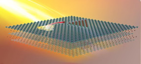 |
| After a monolayer MXene is heated, functional groups are removed from both surfaces. Titanium and carbon atoms migrate from one area to both surfaces, creating a pore and forming new structures. CREDIT Oak Ridge National Laboratory, US Dept. of Energy; image by Xiahan Sang and Andy Sproles. |
Abstract:
Scientists at the Department of Energy's Oak Ridge National Laboratory induced a two-dimensional material to cannibalize itself for atomic "building blocks" from which stable structures formed.
Cannibalistic materials feed on themselves to grow new nanostructures
Oak Ridge, TN | Posted on September 1st, 2018The findings, reported in Nature Communications, provide insights that may improve design of 2D materials for fast-charging energy-storage and electronic devices.
"Under our experimental conditions, titanium and carbon atoms can spontaneously form an atomically thin layer of 2D transition-metal carbide, which was never observed before," said Xiahan Sang of ORNL.
He and ORNL's Raymond Unocic led a team that performed in situ experiments using state-of-the-art scanning transmission electron microscopy (STEM), combined with theory-based simulations, to reveal the mechanism's atomistic details.
"This study is about determining the atomic-level mechanisms and kinetics that are responsible for forming new structures of a 2D transition-metal carbide such that new synthesis methods can be realized for this class of materials," Unocic added.
The starting material was a 2D ceramic called a MXene (pronounced "max een"). Unlike most ceramics, MXenes are good electrical conductors because they are made from alternating atomic layers of carbon or nitrogen sandwiched within transition metals like titanium.
The research was a project of the Fluid Interface Reactions, Structures and Transport (FIRST) Center, a DOE Energy Frontier Research Center that explores fluid-solid interface reactions that have consequences for energy transport in everyday applications. Scientists conducted experiments to synthesize and characterize advanced materials and performed theory and simulation work to explain observed structural and functional properties of the materials. New knowledge from FIRST projects provides guideposts for future studies.
The high-quality material used in these experiments was synthesized by Drexel University scientists, in the form of five-ply single-crystal monolayer flakes of MXene. The flakes were taken from a parent crystal called "MAX," which contains a transition metal denoted by "M"; an element such as aluminum or silicon, denoted by "A"; and either a carbon or nitrogen atom, denoted by "X." The researchers used an acidic solution to etch out the monoatomic aluminum layers, exfoliate the material and delaminate it into individual monolayers of a titanium carbide MXene (Ti3C2).
The ORNL scientists suspended a large MXene flake on a heating chip with holes drilled in it so no support material, or substrate, interfered with the flake. Under vacuum, the suspended flake was exposed to heat and irradiated with an electron beam to clean the MXene surface and fully expose the layer of titanium atoms.
MXenes are typically inert because their surfaces are covered with protective functional groups--oxygen, hydrogen and fluorine atoms that remain after acid exfoliation. After protective groups are removed, the remaining material activates. Atomic-scale defects--"vacancies" created when titanium atoms are removed during etching--are exposed on the outer ply of the monolayer. "These atomic vacancies are good initiation sites," Sang said. "It's favorable for titanium and carbon atoms to move from defective sites to the surface." In an area with a defect, a pore may form when atoms migrate.
"Once those functional groups are gone, now you're left with a bare titanium layer (and underneath, alternating carbon, titanium, carbon, titanium) that's free to reconstruct and form new structures on top of existing structures," Sang said.
High-resolution STEM imaging proved that atoms moved from one part of the material to another to build structures. Because the material feeds on itself, the growth mechanism is cannibalistic.
"The growth mechanism is completely supported by density functional theory and reactive molecular dynamics simulations, thus opening up future possibilities to use these theory tools to determine the experimental parameters required for synthesizing specific defect structures," said Adri van Duin of Penn State.
Most of the time, only one additional layer [of carbon and titanium] grew on a surface. The material changed as atoms built new layers. Ti3C2 turned into Ti4C3, for example.
"These materials are efficient at ionic transport, which lends itself well to battery and supercapacitor applications," Unocic said. "How does ionic transport change when we add more layers to nanometer-thin MXene sheets?" This question may spur future studies.
"Because MXenes containing molybdenum, niobium, vanadium, tantalum, hafnium, chromium and other metals are available, there are opportunities to make a variety of new structures containing more than three or four metal atoms in cross-section (the current limit for MXenes produced from MAX phases)," Yury Gogotsi of Drexel University added. "Those materials may show different useful properties and create an array of 2D building blocks for advancing technology."
At ORNL's Center for Nanophase Materials Sciences (CNMS), Yu Xie, Weiwei Sun and Paul Kent performed first-principles theory calculations to explain why these materials grew layer by layer instead of forming alternate structures, such as squares. Xufan Li and Kai Xiao helped understand the growth mechanism, which minimizes surface energy to stabilize atomic configurations. Penn State scientists conducted large-scale dynamical reactive force field simulations showing how atoms rearranged on surfaces, confirming defect structures and their evolution as observed in experiments.
The researchers hope the new knowledge will help others grow advanced materials and generate useful nanoscale structures.
###
Research was supported as part of the FIRST Center, an Energy Frontier Research Center funded by the U.S. Department of Energy Office of Science. In situ aberration-corrected STEM imaging was conducted at CNMS, a U.S. Department of Energy Office of Science User Facility at ORNL. The research used resources of the National Energy Research Scientific Computing Center, a DOE Office of Science User Facility at Lawrence Berkeley National Laboratory.
####
About Oak Ridge National Laboratory
UT-Battelle manages ORNL for DOE's Office of Science. The single largest supporter of basic research in the physical sciences in the United States, the Office of Science is working to address some of the most pressing challenges of our time. For more information, please visit https://science.energy.gov/. --by Dawn Levy
For more information, please click here
Contacts:
Dawn Levy
865-576-6448
Copyright © Oak Ridge National Laboratory
If you have a comment, please Contact us.Issuers of news releases, not 7th Wave, Inc. or Nanotechnology Now, are solely responsible for the accuracy of the content.
Bookmark:


| Related Links |
| Related News Press |
News and information
![]() Quantum computer improves AI predictions April 17th, 2026
Quantum computer improves AI predictions April 17th, 2026
![]() Flexible sensor gains sensitivity under pressure April 17th, 2026
Flexible sensor gains sensitivity under pressure April 17th, 2026
![]() A reusable chip for particulate matter sensing April 17th, 2026
A reusable chip for particulate matter sensing April 17th, 2026
![]() Detecting vibrational quantum beating in the predissociation dynamics of SF6 using time-resolved photoelectron spectroscopy April 17th, 2026
Detecting vibrational quantum beating in the predissociation dynamics of SF6 using time-resolved photoelectron spectroscopy April 17th, 2026
2 Dimensional Materials
![]() Flexible sensor gains sensitivity under pressure April 17th, 2026
Flexible sensor gains sensitivity under pressure April 17th, 2026
![]() ICFO researchers overcome long-standing bottleneck in single photon detection with twisted 2D materials August 8th, 2025
ICFO researchers overcome long-standing bottleneck in single photon detection with twisted 2D materials August 8th, 2025
![]() First real-time observation of two-dimensional melting process: Researchers at Mainz University unveil new insights into magnetic vortex structures August 8th, 2025
First real-time observation of two-dimensional melting process: Researchers at Mainz University unveil new insights into magnetic vortex structures August 8th, 2025
![]() Lab to industry: InSe wafer-scale breakthrough for future electronics August 8th, 2025
Lab to industry: InSe wafer-scale breakthrough for future electronics August 8th, 2025
Laboratories
![]() Researchers develop molecular qubits that communicate at telecom frequencies October 3rd, 2025
Researchers develop molecular qubits that communicate at telecom frequencies October 3rd, 2025
Govt.-Legislation/Regulation/Funding/Policy
![]() Quantum computer improves AI predictions April 17th, 2026
Quantum computer improves AI predictions April 17th, 2026
![]() Metasurfaces smooth light to boost magnetic sensing precision January 30th, 2026
Metasurfaces smooth light to boost magnetic sensing precision January 30th, 2026
![]() New imaging approach transforms study of bacterial biofilms August 8th, 2025
New imaging approach transforms study of bacterial biofilms August 8th, 2025
Possible Futures
![]() A fundamentally new therapeutic approach to cystic fibrosis: Nanobody repairs cellular defect April 17th, 2026
A fundamentally new therapeutic approach to cystic fibrosis: Nanobody repairs cellular defect April 17th, 2026
![]() UC Irvine physicists discover method to reverse �quantum scrambling� : The work addresses the problem of information loss in quantum computing system April 17th, 2026
UC Irvine physicists discover method to reverse �quantum scrambling� : The work addresses the problem of information loss in quantum computing system April 17th, 2026
Chip Technology
![]() A reusable chip for particulate matter sensing April 17th, 2026
A reusable chip for particulate matter sensing April 17th, 2026
![]() Metasurfaces smooth light to boost magnetic sensing precision January 30th, 2026
Metasurfaces smooth light to boost magnetic sensing precision January 30th, 2026
Nanoelectronics
![]() Lab to industry: InSe wafer-scale breakthrough for future electronics August 8th, 2025
Lab to industry: InSe wafer-scale breakthrough for future electronics August 8th, 2025
![]() Interdisciplinary: Rice team tackles the future of semiconductors Multiferroics could be the key to ultralow-energy computing October 6th, 2023
Interdisciplinary: Rice team tackles the future of semiconductors Multiferroics could be the key to ultralow-energy computing October 6th, 2023
![]() Key element for a scalable quantum computer: Physicists from Forschungszentrum J�lich and RWTH Aachen University demonstrate electron transport on a quantum chip September 23rd, 2022
Key element for a scalable quantum computer: Physicists from Forschungszentrum J�lich and RWTH Aachen University demonstrate electron transport on a quantum chip September 23rd, 2022
![]() Reduced power consumption in semiconductor devices September 23rd, 2022
Reduced power consumption in semiconductor devices September 23rd, 2022
Discoveries
![]() Quantum computer improves AI predictions April 17th, 2026
Quantum computer improves AI predictions April 17th, 2026
![]() Flexible sensor gains sensitivity under pressure April 17th, 2026
Flexible sensor gains sensitivity under pressure April 17th, 2026
![]() A reusable chip for particulate matter sensing April 17th, 2026
A reusable chip for particulate matter sensing April 17th, 2026
![]() Detecting vibrational quantum beating in the predissociation dynamics of SF6 using time-resolved photoelectron spectroscopy April 17th, 2026
Detecting vibrational quantum beating in the predissociation dynamics of SF6 using time-resolved photoelectron spectroscopy April 17th, 2026
Materials/Metamaterials/Magnetoresistance
![]() First real-time observation of two-dimensional melting process: Researchers at Mainz University unveil new insights into magnetic vortex structures August 8th, 2025
First real-time observation of two-dimensional melting process: Researchers at Mainz University unveil new insights into magnetic vortex structures August 8th, 2025
![]() Researchers unveil a groundbreaking clay-based solution to capture carbon dioxide and combat climate change June 6th, 2025
Researchers unveil a groundbreaking clay-based solution to capture carbon dioxide and combat climate change June 6th, 2025
![]() A 1960s idea inspires NBI researchers to study hitherto inaccessible quantum states June 6th, 2025
A 1960s idea inspires NBI researchers to study hitherto inaccessible quantum states June 6th, 2025
![]() Institute for Nanoscience hosts annual proposal planning meeting May 16th, 2025
Institute for Nanoscience hosts annual proposal planning meeting May 16th, 2025
Announcements
![]() A fundamentally new therapeutic approach to cystic fibrosis: Nanobody repairs cellular defect April 17th, 2026
A fundamentally new therapeutic approach to cystic fibrosis: Nanobody repairs cellular defect April 17th, 2026
![]() UC Irvine physicists discover method to reverse �quantum scrambling� : The work addresses the problem of information loss in quantum computing system April 17th, 2026
UC Irvine physicists discover method to reverse �quantum scrambling� : The work addresses the problem of information loss in quantum computing system April 17th, 2026
Interviews/Book Reviews/Essays/Reports/Podcasts/Journals/White papers/Posters
![]() A fundamentally new therapeutic approach to cystic fibrosis: Nanobody repairs cellular defect April 17th, 2026
A fundamentally new therapeutic approach to cystic fibrosis: Nanobody repairs cellular defect April 17th, 2026
![]() UC Irvine physicists discover method to reverse �quantum scrambling� : The work addresses the problem of information loss in quantum computing system April 17th, 2026
UC Irvine physicists discover method to reverse �quantum scrambling� : The work addresses the problem of information loss in quantum computing system April 17th, 2026
Battery Technology/Capacitors/Generators/Piezoelectrics/Thermoelectrics/Energy storage
![]() Decoding hydrogen‑bond network of electrolyte for cryogenic durable aqueous zinc‑ion batteries January 30th, 2026
Decoding hydrogen‑bond network of electrolyte for cryogenic durable aqueous zinc‑ion batteries January 30th, 2026
![]() COF scaffold membrane with gate‑lane nanostructure for efficient Li+/Mg2+ separation January 30th, 2026
COF scaffold membrane with gate‑lane nanostructure for efficient Li+/Mg2+ separation January 30th, 2026
![]() MXene nanomaterials enter a new dimension Multilayer nanomaterial: MXene flakes created at Drexel University show new promise as 1D scrolls January 30th, 2026
MXene nanomaterials enter a new dimension Multilayer nanomaterial: MXene flakes created at Drexel University show new promise as 1D scrolls January 30th, 2026
Research partnerships
![]() Lab to industry: InSe wafer-scale breakthrough for future electronics August 8th, 2025
Lab to industry: InSe wafer-scale breakthrough for future electronics August 8th, 2025
![]() HKU physicists uncover hidden order in the quantum world through deconfined quantum critical points April 25th, 2025
HKU physicists uncover hidden order in the quantum world through deconfined quantum critical points April 25th, 2025
|
|
||
|
|
||
| The latest news from around the world, FREE | ||
|
|
||
|
|
||
| Premium Products | ||
|
|
||
|
Only the news you want to read!
Learn More |
||
|
|
||
|
Full-service, expert consulting
Learn More |
||
|
|
||