Home > Press > Building nanomaterials for next-generation computing: Scientists recently developed a blueprint to fabricate new nanoheterostructures using 2D materials
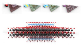 |
| Nanoscientists at Northwestern University have developed a blueprint to fabricate new heterostructures from different types of 2-D materials. The researchers describe their blueprint in the Journal of Applied Physics. In this image: Top: Vertical MoSe2-WSe2 heterostructure, radial MoS2-WS2 heterostructure, hybrid MoS2-WS2 heterostructure and Mose2-WSe2 alloy building block representations and crystal structure models Bottom: Vertical MoSe2-WSe2 heterostructure crystal structure model CREDIT Cain, Hanson and Dravid |
Abstract:
Nanoscientists at Northwestern University have developed a blueprint to fabricate new heterostructures from different types of 2-D materials. 2-D materials are single atom layers that can be stacked together like "nano-interlocking building blocks." Materials scientists and physicists are excited about the properties of 2-D materials and their potential applications. The researchers describe their blueprint in the Journal of Applied Physics, from AIP Publishing.
Building nanomaterials for next-generation computing: Scientists recently developed a blueprint to fabricate new nanoheterostructures using 2D materials
Washington, DC | Posted on June 1st, 2018"We've outlined an easy, deterministic and readily deployable way to stack and stitch these individual layers into orders not seen in nature," said Jeffrey Cain, an author on the paper who was formerly at Northwestern University but is now at Lawrence Berkeley National Laboratory and the University of California.
Cain explained that for nanoscientists, "the dream" is to combine 2-D materials in any order and collate a library of these heterostructures with their documented properties. Scientists can then select appropriate heterostructures from the library for their desired applications. For instance, the computer industry is trying to make transistors smaller and faster to increase computing power. A nanoscale semiconductor with favorable electronic properties could be used to make transistors in next-generation computers.
So far, nanoscientists have lacked clear methods for fabricating heterostructures, and have not yet been able to develop this library. In this work, the scientists looked to solve these fabrication issues. After identifying trends in the literature, they tested different conditions to map out the different parameters required to grow specific heterostructures from four types of 2-D materials: molybdenum disulfide and diselenide, and tungsten disulfide and diselenide. To fully characterize the atomically thin final products, the scientists used microscopy and spectrometry techniques.
The group was inspired by the science of time-temperature-transformation diagrams in classical materials, which maps out heating and cooling profiles to generate precise metallic microstructures. Based on this method, the researchers packaged their findings into one diagrammatic technique -- the Time-Temperature-Architecture Diagram.
"People had previously written papers for specific morphologies, but we have unified it all and enabled the generation of these morphologies with one technique," Cain said.
The unified Time-Temperature-Architecture Diagrams provide directions for the exact conditions required to generate numerous heterostructure morphologies and compositions. Using these diagrams, the researchers developed a unique library of nanostructures with physical properties of interest to physicists and materials scientists. The Northwestern University scientists are now examining the behaviors displayed by some materials in their library, like the electron flow across the stitched junctions between materials.
The researchers hope that their blueprint design will be useful for heterostructure fabrication beyond the first four materials. "Our specific diagrams would need revisions in the context of each new material, but we think that this idea is applicable and extendable to other material systems," Cain said.
####
About American Institute of Physics
Journal of Applied Physics is an influential international journal publishing significant new experimental and theoretical results of applied physics research. See http://jap.aip.org .
For more information, please click here
Contacts:
Julia Majors
301-209-3090
Copyright © American Institute of Physics
If you have a comment, please Contact us.Issuers of news releases, not 7th Wave, Inc. or Nanotechnology Now, are solely responsible for the accuracy of the content.
Bookmark:


| Related Links |
| Related News Press |
News and information
![]() Quantum computer improves AI predictions April 17th, 2026
Quantum computer improves AI predictions April 17th, 2026
![]() Flexible sensor gains sensitivity under pressure April 17th, 2026
Flexible sensor gains sensitivity under pressure April 17th, 2026
![]() A reusable chip for particulate matter sensing April 17th, 2026
A reusable chip for particulate matter sensing April 17th, 2026
![]() Detecting vibrational quantum beating in the predissociation dynamics of SF6 using time-resolved photoelectron spectroscopy April 17th, 2026
Detecting vibrational quantum beating in the predissociation dynamics of SF6 using time-resolved photoelectron spectroscopy April 17th, 2026
2 Dimensional Materials
![]() Flexible sensor gains sensitivity under pressure April 17th, 2026
Flexible sensor gains sensitivity under pressure April 17th, 2026
![]() ICFO researchers overcome long-standing bottleneck in single photon detection with twisted 2D materials August 8th, 2025
ICFO researchers overcome long-standing bottleneck in single photon detection with twisted 2D materials August 8th, 2025
![]() First real-time observation of two-dimensional melting process: Researchers at Mainz University unveil new insights into magnetic vortex structures August 8th, 2025
First real-time observation of two-dimensional melting process: Researchers at Mainz University unveil new insights into magnetic vortex structures August 8th, 2025
![]() Lab to industry: InSe wafer-scale breakthrough for future electronics August 8th, 2025
Lab to industry: InSe wafer-scale breakthrough for future electronics August 8th, 2025
Laboratories
![]() Researchers develop molecular qubits that communicate at telecom frequencies October 3rd, 2025
Researchers develop molecular qubits that communicate at telecom frequencies October 3rd, 2025
Hardware
![]() The present and future of computing get a boost from new research July 21st, 2023
The present and future of computing get a boost from new research July 21st, 2023
![]() A Carbon Nanotube Microprocessor Mature Enough to Say Hello: Three new breakthroughs make commercial nanotube processors possible March 2nd, 2020
A Carbon Nanotube Microprocessor Mature Enough to Say Hello: Three new breakthroughs make commercial nanotube processors possible March 2nd, 2020
![]() Powering the future: Smallest all-digital circuit opens doors to 5 nm next-gen semiconductor February 11th, 2020
Powering the future: Smallest all-digital circuit opens doors to 5 nm next-gen semiconductor February 11th, 2020
Possible Futures
![]() A fundamentally new therapeutic approach to cystic fibrosis: Nanobody repairs cellular defect April 17th, 2026
A fundamentally new therapeutic approach to cystic fibrosis: Nanobody repairs cellular defect April 17th, 2026
![]() UC Irvine physicists discover method to reverse �quantum scrambling� : The work addresses the problem of information loss in quantum computing system April 17th, 2026
UC Irvine physicists discover method to reverse �quantum scrambling� : The work addresses the problem of information loss in quantum computing system April 17th, 2026
Chip Technology
![]() A reusable chip for particulate matter sensing April 17th, 2026
A reusable chip for particulate matter sensing April 17th, 2026
![]() Metasurfaces smooth light to boost magnetic sensing precision January 30th, 2026
Metasurfaces smooth light to boost magnetic sensing precision January 30th, 2026
Nanoelectronics
![]() Lab to industry: InSe wafer-scale breakthrough for future electronics August 8th, 2025
Lab to industry: InSe wafer-scale breakthrough for future electronics August 8th, 2025
![]() Interdisciplinary: Rice team tackles the future of semiconductors Multiferroics could be the key to ultralow-energy computing October 6th, 2023
Interdisciplinary: Rice team tackles the future of semiconductors Multiferroics could be the key to ultralow-energy computing October 6th, 2023
![]() Key element for a scalable quantum computer: Physicists from Forschungszentrum J�lich and RWTH Aachen University demonstrate electron transport on a quantum chip September 23rd, 2022
Key element for a scalable quantum computer: Physicists from Forschungszentrum J�lich and RWTH Aachen University demonstrate electron transport on a quantum chip September 23rd, 2022
![]() Reduced power consumption in semiconductor devices September 23rd, 2022
Reduced power consumption in semiconductor devices September 23rd, 2022
Materials/Metamaterials/Magnetoresistance
![]() First real-time observation of two-dimensional melting process: Researchers at Mainz University unveil new insights into magnetic vortex structures August 8th, 2025
First real-time observation of two-dimensional melting process: Researchers at Mainz University unveil new insights into magnetic vortex structures August 8th, 2025
![]() Researchers unveil a groundbreaking clay-based solution to capture carbon dioxide and combat climate change June 6th, 2025
Researchers unveil a groundbreaking clay-based solution to capture carbon dioxide and combat climate change June 6th, 2025
![]() A 1960s idea inspires NBI researchers to study hitherto inaccessible quantum states June 6th, 2025
A 1960s idea inspires NBI researchers to study hitherto inaccessible quantum states June 6th, 2025
![]() Institute for Nanoscience hosts annual proposal planning meeting May 16th, 2025
Institute for Nanoscience hosts annual proposal planning meeting May 16th, 2025
Announcements
![]() A fundamentally new therapeutic approach to cystic fibrosis: Nanobody repairs cellular defect April 17th, 2026
A fundamentally new therapeutic approach to cystic fibrosis: Nanobody repairs cellular defect April 17th, 2026
![]() UC Irvine physicists discover method to reverse �quantum scrambling� : The work addresses the problem of information loss in quantum computing system April 17th, 2026
UC Irvine physicists discover method to reverse �quantum scrambling� : The work addresses the problem of information loss in quantum computing system April 17th, 2026
Interviews/Book Reviews/Essays/Reports/Podcasts/Journals/White papers/Posters
![]() A fundamentally new therapeutic approach to cystic fibrosis: Nanobody repairs cellular defect April 17th, 2026
A fundamentally new therapeutic approach to cystic fibrosis: Nanobody repairs cellular defect April 17th, 2026
![]() UC Irvine physicists discover method to reverse �quantum scrambling� : The work addresses the problem of information loss in quantum computing system April 17th, 2026
UC Irvine physicists discover method to reverse �quantum scrambling� : The work addresses the problem of information loss in quantum computing system April 17th, 2026
|
|
||
|
|
||
| The latest news from around the world, FREE | ||
|
|
||
|
|
||
| Premium Products | ||
|
|
||
|
Only the news you want to read!
Learn More |
||
|
|
||
|
Full-service, expert consulting
Learn More |
||
|
|
||