Home > Press > NIST Puts the Optical Microscope Under the Microscope to Achieve Atomic Accuracy
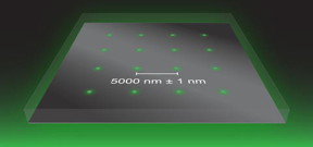 |
| Illustration shows an array of apertures with a spacing of 5000 nanometers (nm) ± 1 nm. The apertures pass light through a metal film on a glass slide. Imaging the aperture array with an optical microscope results in apparent errors in the spacing between apertures. Knowledge of the true spacing allows correction of these imaging errors. This calibration process enables accurate measurements of position across a large image. Credit: NIST |
Abstract:
Over the last two decades, scientists have discovered that the optical microscope can be used to detect, track and image objects much smaller than their traditional limit—about half the wavelength of visible light, or a few hundred nanometers.
NIST Puts the Optical Microscope Under the Microscope to Achieve Atomic Accuracy
Gaithersburg, MD | Posted on May 22nd, 2018That pioneering research, which won the 2014 Nobel Prize in Chemistry, has enabled researchers to track proteins in fertilized eggs, visualize how molecules form electrical connections between nerve cells in the brain, and study the nanoscale motion of miniature motors.
Now, research developments at the National Institute of Standards and Technology (NIST) enable the microscopes to measure these nanometer-scale details with a new level of accuracy.
“We put the optical microscope under a microscope to achieve accuracy near the atomic scale,” said NIST’s Samuel Stavis, who served as the project leader for these efforts.
Because optical microscopes have not traditionally been used to study the nanometer scale, they typically lack the calibration—comparison to a standard to check that a result is correct—necessary to obtain information that is accurate at that scale. A microscope may be precise, consistently indicating the same position for a single molecule or nanoparticle. Yet, at the same time, it can be highly inaccurate—the location of the object identified by the microscope to within a billionth of a meter may, in fact, be millionths of a meter off due to unaccounted-for errors. “Precision without accuracy can be very misleading,” said Jon Geist, a NIST co-author of the study.
To address the problem, NIST has developed a new calibration process that closely examines and corrects these imaging errors. The process uses reference materials—objects with characteristics that are well-known and stable—that have the potential for mass production and widespread distribution to individual laboratories.
This is important because optical microscopes are common laboratory instruments that can easily magnify different samples, ranging from delicate biological specimens to electrical and mechanical devices. As well, optical microscopes are becoming increasingly capable and economical as they incorporate scientific versions of the lights and cameras in smartphones.
The NIST team relied on nanometer-scale fabrication processes to develop the reference material. The researchers used electron beams and ion milling to form an array of pinhole apertures through a thin film of platinum on a glass slide. The process enabled the team to space the apertures 5,000 nanometers apart, to within an accuracy of about 1 nanometer. In this way, the researchers built a measure of accuracy into the aperture positions.
Shining light through the array of apertures creates an array of points for imaging. But because all microscope lenses have imperfections, errors inevitably occur during imaging that change the apparent positions of the points, making the spacing between the apertures appear to be larger or smaller than the actual spacing engineered by the team. Knowledge of the true spacing allows correction of the imaging errors and calibration of the microscope for measurements of position with high accuracy across a wide field of view.
Even a small error can lead to a large problem. Consider, for example, a microscope having an actual magnification of 103 times when the expected magnification, as specified by the manufacturer, is 100 times. The resulting error of 3 percent adds up over large distances across a microscope image. Because of lens imperfections, a subtler problem also occurs—the microscope magnification changes across the image, causing image distortion. To solve this problem, the NIST team designed aperture arrays and calibration processes that worked across large fields of view.
The aperture arrays, which would enable individual researchers to perform calibrations in their own laboratories, could improve by a factor of 10,000 the ability of optical microscopes to accurately locate the position of single molecules and nanoparticles.
Stavis and his colleagues, including first author Craig Copeland of NIST and the Maryland NanoCenter at the University of Maryland, reported their findings in a recently posted article (link is external) in Light: Science & Applications.
“We have identified and solved an underappreciated problem,” said Copeland.
Having calibrated their optical microscope using the arrays, the team reversed the process, using their microscope to identify imperfections in the prototype arrays from the nanofabrication process. “We tested the limits of nanofabrication to control the aperture spacing,” noted co-author Rob Ilic, manager of NIST’s NanoFab. The ease and speed of optical microscopy could facilitate quality control of aperture arrays in a production process.
Finally, the team exploited the inherent stability of the aperture arrays to evaluate whether fluorescent nanoparticles, often used as fixed points of reference in optical microscopy, actually remained fixed to a particular point or if they moved around. The researchers found that while unintentional motions of their optical microscope made views of the nanoparticles blurry, using the aperture array showed that the nanoparticles were not actually moving at atomic scales.
####
For more information, please click here
Contacts:
Ben P. Stein
(link sends e-mail)
(301) 975-2763
Copyright © National Institute of Standards and Technology (NIST)
If you have a comment, please Contact us.Issuers of news releases, not 7th Wave, Inc. or Nanotechnology Now, are solely responsible for the accuracy of the content.
Bookmark:


| Related Links |
| Related News Press |
News and information
![]() Quantum computer improves AI predictions April 17th, 2026
Quantum computer improves AI predictions April 17th, 2026
![]() Flexible sensor gains sensitivity under pressure April 17th, 2026
Flexible sensor gains sensitivity under pressure April 17th, 2026
![]() A reusable chip for particulate matter sensing April 17th, 2026
A reusable chip for particulate matter sensing April 17th, 2026
![]() Detecting vibrational quantum beating in the predissociation dynamics of SF6 using time-resolved photoelectron spectroscopy April 17th, 2026
Detecting vibrational quantum beating in the predissociation dynamics of SF6 using time-resolved photoelectron spectroscopy April 17th, 2026
Imaging
![]() Simple algorithm paired with standard imaging tool could predict failure in lithium metal batteries August 8th, 2025
Simple algorithm paired with standard imaging tool could predict failure in lithium metal batteries August 8th, 2025
![]() First real-time observation of two-dimensional melting process: Researchers at Mainz University unveil new insights into magnetic vortex structures August 8th, 2025
First real-time observation of two-dimensional melting process: Researchers at Mainz University unveil new insights into magnetic vortex structures August 8th, 2025
![]() New imaging approach transforms study of bacterial biofilms August 8th, 2025
New imaging approach transforms study of bacterial biofilms August 8th, 2025
Laboratories
![]() Researchers develop molecular qubits that communicate at telecom frequencies October 3rd, 2025
Researchers develop molecular qubits that communicate at telecom frequencies October 3rd, 2025
Govt.-Legislation/Regulation/Funding/Policy
![]() Quantum computer improves AI predictions April 17th, 2026
Quantum computer improves AI predictions April 17th, 2026
![]() Metasurfaces smooth light to boost magnetic sensing precision January 30th, 2026
Metasurfaces smooth light to boost magnetic sensing precision January 30th, 2026
![]() New imaging approach transforms study of bacterial biofilms August 8th, 2025
New imaging approach transforms study of bacterial biofilms August 8th, 2025
Possible Futures
![]() A fundamentally new therapeutic approach to cystic fibrosis: Nanobody repairs cellular defect April 17th, 2026
A fundamentally new therapeutic approach to cystic fibrosis: Nanobody repairs cellular defect April 17th, 2026
![]() UC Irvine physicists discover method to reverse ‘quantum scrambling’ : The work addresses the problem of information loss in quantum computing system April 17th, 2026
UC Irvine physicists discover method to reverse ‘quantum scrambling’ : The work addresses the problem of information loss in quantum computing system April 17th, 2026
Discoveries
![]() Quantum computer improves AI predictions April 17th, 2026
Quantum computer improves AI predictions April 17th, 2026
![]() Flexible sensor gains sensitivity under pressure April 17th, 2026
Flexible sensor gains sensitivity under pressure April 17th, 2026
![]() A reusable chip for particulate matter sensing April 17th, 2026
A reusable chip for particulate matter sensing April 17th, 2026
![]() Detecting vibrational quantum beating in the predissociation dynamics of SF6 using time-resolved photoelectron spectroscopy April 17th, 2026
Detecting vibrational quantum beating in the predissociation dynamics of SF6 using time-resolved photoelectron spectroscopy April 17th, 2026
Announcements
![]() A fundamentally new therapeutic approach to cystic fibrosis: Nanobody repairs cellular defect April 17th, 2026
A fundamentally new therapeutic approach to cystic fibrosis: Nanobody repairs cellular defect April 17th, 2026
![]() UC Irvine physicists discover method to reverse ‘quantum scrambling’ : The work addresses the problem of information loss in quantum computing system April 17th, 2026
UC Irvine physicists discover method to reverse ‘quantum scrambling’ : The work addresses the problem of information loss in quantum computing system April 17th, 2026
Interviews/Book Reviews/Essays/Reports/Podcasts/Journals/White papers/Posters
![]() A fundamentally new therapeutic approach to cystic fibrosis: Nanobody repairs cellular defect April 17th, 2026
A fundamentally new therapeutic approach to cystic fibrosis: Nanobody repairs cellular defect April 17th, 2026
![]() UC Irvine physicists discover method to reverse ‘quantum scrambling’ : The work addresses the problem of information loss in quantum computing system April 17th, 2026
UC Irvine physicists discover method to reverse ‘quantum scrambling’ : The work addresses the problem of information loss in quantum computing system April 17th, 2026
Tools
![]() Metasurfaces smooth light to boost magnetic sensing precision January 30th, 2026
Metasurfaces smooth light to boost magnetic sensing precision January 30th, 2026
![]() From sensors to smart systems: the rise of AI-driven photonic noses January 30th, 2026
From sensors to smart systems: the rise of AI-driven photonic noses January 30th, 2026
![]() Japan launches fully domestically produced quantum computer: Expo visitors to experience quantum computing firsthand August 8th, 2025
Japan launches fully domestically produced quantum computer: Expo visitors to experience quantum computing firsthand August 8th, 2025
Research partnerships
![]() Lab to industry: InSe wafer-scale breakthrough for future electronics August 8th, 2025
Lab to industry: InSe wafer-scale breakthrough for future electronics August 8th, 2025
![]() HKU physicists uncover hidden order in the quantum world through deconfined quantum critical points April 25th, 2025
HKU physicists uncover hidden order in the quantum world through deconfined quantum critical points April 25th, 2025
|
|
||
|
|
||
| The latest news from around the world, FREE | ||
|
|
||
|
|
||
| Premium Products | ||
|
|
||
|
Only the news you want to read!
Learn More |
||
|
|
||
|
Full-service, expert consulting
Learn More |
||
|
|
||