Home > Press > High-speed and on-silicon-chip graphene blackbody emitters: Integrated light emitters for optical communications
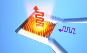 |
| Square graphene sheet is connected to source and drain electrodes. Modulated blackbody emission is obtained from graphene by applying input signal. CREDIT Keio University |
Abstract:
Graphene is a two-dimensional nanocarbon material, having unique properties in electronic, optical and thermal properties, which can be applied for optoelectronic devices. Graphene-based blackbody emitters are also promising light emitters on silicon chip in NIR and mid-infrared region. However, although graphene-based blackbody emitters have been demonstrated under steady-state conditions or relatively slow modulation (100 kHz), the transient properties of these emitters under high-speed modulation have not been reported to date. Also, the optical communications with graphene-based emitters have never been demonstrated.
High-speed and on-silicon-chip graphene blackbody emitters: Integrated light emitters for optical communications
Tokyo, Japan | Posted on April 5th, 2018Here, a highly integrated, high-speed and on-chip blackbody emitter based on graphene in NIR region including telecommunication wavelength was demonstrated. A fast response time of ~ 100 ps, which is ~ 105 higher than the previous graphene emitters, has been experimentally demonstrated for single and few-layer graphene, the emission responses can be controlled by the graphene contact with the substrate depending on the number of graphene layers. The mechanisms of the high-speed emission are elucidated by performing theoretical calculations of the heat conduction equations considering the thermal model of emitters including graphene and a substrate. The simulated results indicate that the fast response properties can be understood not only by the classical thermal transport of in-plane heat conduction in graphene and heat dissipation to the substrate but also by the remote quantum thermal transport via the surface polar phonons (SPoPhs) of the substrates. In addition, first real-time optical communication with graphene-based light emitters was experimentally demonstrated, indicating that graphene emitters are novel light sources for optical communication. Furthermore, we fabricated integrated two-dimensional array emitters with large-scale graphene grown by chemical vapour deposition (CVD) method and capped emitters operable in air, and carried out the direct coupling of optical fibers to the emitters owing to their small footprint and planar device structure.
Graphene light emitters are greatly advantageous over conventional compound semiconductor emitters because they can be highly integrated on silicon chip due to simple fabrication processes of graphene emitters and direct coupling with silicon waveguide through an evanescent field. Because graphene can realize high-speed, small footprint and on-Si-chip light emitters, which are still challenges for compound semiconductors, the graphene-based light emitters can open new routes to highly integrated optoelectronics and silicon photonics.
####
For more information, please click here
Contacts:
Hideyuki Maki
81-455-661-643
Copyright © Japan Science and Technology Agency
If you have a comment, please Contact us.Issuers of news releases, not 7th Wave, Inc. or Nanotechnology Now, are solely responsible for the accuracy of the content.
Bookmark:


| Related Links |
| Related News Press |
News and information
![]() Quantum computer improves AI predictions April 17th, 2026
Quantum computer improves AI predictions April 17th, 2026
![]() Flexible sensor gains sensitivity under pressure April 17th, 2026
Flexible sensor gains sensitivity under pressure April 17th, 2026
![]() A reusable chip for particulate matter sensing April 17th, 2026
A reusable chip for particulate matter sensing April 17th, 2026
![]() Detecting vibrational quantum beating in the predissociation dynamics of SF6 using time-resolved photoelectron spectroscopy April 17th, 2026
Detecting vibrational quantum beating in the predissociation dynamics of SF6 using time-resolved photoelectron spectroscopy April 17th, 2026
Wireless/telecommunications/RF/Antennas/Microwaves
![]() Researchers develop molecular qubits that communicate at telecom frequencies October 3rd, 2025
Researchers develop molecular qubits that communicate at telecom frequencies October 3rd, 2025
Graphene/ Graphite
![]() Electrifying results shed light on graphene foam as a potential material for lab grown cartilage June 6th, 2025
Electrifying results shed light on graphene foam as a potential material for lab grown cartilage June 6th, 2025
![]() Breakthrough in proton barrier films using pore-free graphene oxide: Kumamoto University researchers achieve new milestone in advanced coating technologies September 13th, 2024
Breakthrough in proton barrier films using pore-free graphene oxide: Kumamoto University researchers achieve new milestone in advanced coating technologies September 13th, 2024
Chip Technology
![]() A reusable chip for particulate matter sensing April 17th, 2026
A reusable chip for particulate matter sensing April 17th, 2026
![]() Metasurfaces smooth light to boost magnetic sensing precision January 30th, 2026
Metasurfaces smooth light to boost magnetic sensing precision January 30th, 2026
Optical computing/Photonic computing
![]() ICFO researchers overcome long-standing bottleneck in single photon detection with twisted 2D materials August 8th, 2025
ICFO researchers overcome long-standing bottleneck in single photon detection with twisted 2D materials August 8th, 2025
![]() Programmable electron-induced color router array May 14th, 2025
Programmable electron-induced color router array May 14th, 2025
Announcements
![]() A fundamentally new therapeutic approach to cystic fibrosis: Nanobody repairs cellular defect April 17th, 2026
A fundamentally new therapeutic approach to cystic fibrosis: Nanobody repairs cellular defect April 17th, 2026
![]() UC Irvine physicists discover method to reverse �quantum scrambling� : The work addresses the problem of information loss in quantum computing system April 17th, 2026
UC Irvine physicists discover method to reverse �quantum scrambling� : The work addresses the problem of information loss in quantum computing system April 17th, 2026
Photonics/Optics/Lasers
![]() Metasurfaces smooth light to boost magnetic sensing precision January 30th, 2026
Metasurfaces smooth light to boost magnetic sensing precision January 30th, 2026
![]() From sensors to smart systems: the rise of AI-driven photonic noses January 30th, 2026
From sensors to smart systems: the rise of AI-driven photonic noses January 30th, 2026
|
|
||
|
|
||
| The latest news from around the world, FREE | ||
|
|
||
|
|
||
| Premium Products | ||
|
|
||
|
Only the news you want to read!
Learn More |
||
|
|
||
|
Full-service, expert consulting
Learn More |
||
|
|
||