Home > Press > UCLA researchers develop a new class of two-dimensional materials: New kinds of 'superlattices' could lead to improvements in electronics, from transistors to LEDs
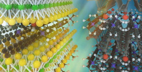 |
| This is an artist's concept of two kinds of monolayer atomic crystal molecular superlattices. On the left, molybdenum disulfide with layers of ammonium molecules, on the right, black phosphorus with layers of ammonium molecules. CREDIT UCLA Samueli Engineering |
Abstract:
A research team led by UCLA scientists and engineers has developed a method to make new kinds of artificial "superlattices" -- materials comprised of alternating layers of ultra-thin "two-dimensional" sheets, which are only one or a few atoms thick. Unlike current state-of-the art superlattices, in which alternating layers have similar atomic structures, and thus similar electronic properties, these alternating layers can have radically different structures, properties and functions, something not previously available.
UCLA researchers develop a new class of two-dimensional materials: New kinds of 'superlattices' could lead to improvements in electronics, from transistors to LEDs
Los Angeles, CA | Posted on March 11th, 2018For example, while one layer of this new kind of superlattice can allow a fast flow of electrons through it, the other type of layer can act as an insulator. This design confines the electronic and optical properties to single active layers, and prevents them from interfering with other insulating layers.
Such superlattices can form the basis for improved and new classes of electronic and optoelectronic devices. Applications include superfast and ultra-efficient semiconductors for transistors in computers and smart devices, and advanced LEDs and lasers.
Compared with the conventional layer-by-layer assembly or growth approach currently used to create 2D superlattices, the new UCLA-led process to manufacture superlattices from 2D materials is much faster and more efficient. Most importantly, the new method easily yields superlattices with tens, hundreds or even thousands of alternating layers, which is not yet possible with other approaches.
This new class of superlattices alternates 2D atomic crystal sheets that are interspaced with molecules of varying shapes and sizes. In effect, this molecular layer becomes the second "sheet" because it is held in place by "van der Waals" forces, weak electrostatic forces to keep otherwise neutral molecules "attached" to each other. These new superlattices are called "monolayer atomic crystal molecular superlattices."
The study, published in Nature, was led by Xiangfeng Duan, UCLA professor of chemistry and biochemistry, and Yu Huang, UCLA professor of materials science and engineering at the UCLA Samueli School of Engineering.
"Traditional semiconductor superlattices can usually only be made from materials with highly similar lattice symmetry, normally with rather similar electronic structures," Huang said. "For the first time, we have created stable superlattice structures with radically different layers, yet nearly perfect atomic-molecular arrangements within each layer. This new class of superlattice structures has tailorable electronic properties for potential technological applications and further scientific studies."
One current method to build a superlattice is to manually stack the ultrathin layers one on top of the other. But this is labor-intensive. In addition, since the flake-like sheets are fragile, it takes a long time to build because many sheets will break during the placement process. The other method is to grow one new layer on top of the other, using a process called "chemical vapor deposition." But since that means different conditions, such as heat, pressure or chemical environments, are needed to grow each layer, the process could result in altering or breaking the layer underneath. This method is also labor-intensive with low yield rates.
The new method to create monolayer atomic crystal molecular superlattices uses a process called "electrochemical intercalation," in which a negative voltage is applied. This injects negatively charged electrons into the 2D material. Then, this attracts positively charged ammonium molecules into the spaces between the atomic layers. Those ammonium molecules automatically assemble into new layers in the ordered crystal structure, creating a superlattice.
"Think of a two-dimensional material as a stack of playing cards," Duan said. "Then imagine that we can cause a large pile of nearby plastic beads to insert themselves, in perfect order, sandwiching between each card. That's the analogous idea, but with a crystal of 2D material and ammonium molecules."
The researchers first demonstrated the new technique using black phosphorus as a base 2D atomic crystal material. Using the negative voltage, positively charged ammonium ions were attracted into the base material, and inserted themselves between the layered atomic phosphorous sheets."
Following that success, the team inserted different types of ammonium molecules with various sizes and symmetries into a series of 2D materials to create a broad class of superlattices. They found that they could tailor the structures of the resulting monolayer atomic crystal molecular superlattices, which had a diverse range of desirable electronic and optical properties."The resulting materials could be useful for making faster transistors that consume less power, or for creating efficient light-emitting devices," Duan said.
###
The lead author of the study is Chen Wang, a doctoral student advised by Huang and Duan. Other study authors are UCLA graduate students and postdoctoral researchers in Duan or Huang's research groups; researchers from Caltech; Hunan University, China; University of Science and Technology of China; and King Saud University, Saudi Arabia.
The research was supported by the National Science Foundation and the Office of Naval Research.
####
For more information, please click here
Contacts:
Amy Akmal
310-429-8689
Copyright © UCLA
If you have a comment, please Contact us.Issuers of news releases, not 7th Wave, Inc. or Nanotechnology Now, are solely responsible for the accuracy of the content.
Bookmark:


| Related News Press |
News and information
![]() Quantum computer improves AI predictions April 17th, 2026
Quantum computer improves AI predictions April 17th, 2026
![]() Flexible sensor gains sensitivity under pressure April 17th, 2026
Flexible sensor gains sensitivity under pressure April 17th, 2026
![]() A reusable chip for particulate matter sensing April 17th, 2026
A reusable chip for particulate matter sensing April 17th, 2026
![]() Detecting vibrational quantum beating in the predissociation dynamics of SF6 using time-resolved photoelectron spectroscopy April 17th, 2026
Detecting vibrational quantum beating in the predissociation dynamics of SF6 using time-resolved photoelectron spectroscopy April 17th, 2026
2 Dimensional Materials
![]() Flexible sensor gains sensitivity under pressure April 17th, 2026
Flexible sensor gains sensitivity under pressure April 17th, 2026
Govt.-Legislation/Regulation/Funding/Policy
![]() Quantum computer improves AI predictions April 17th, 2026
Quantum computer improves AI predictions April 17th, 2026
![]() Metasurfaces smooth light to boost magnetic sensing precision January 30th, 2026
Metasurfaces smooth light to boost magnetic sensing precision January 30th, 2026
![]() New imaging approach transforms study of bacterial biofilms August 8th, 2025
New imaging approach transforms study of bacterial biofilms August 8th, 2025
Possible Futures
![]() A fundamentally new therapeutic approach to cystic fibrosis: Nanobody repairs cellular defect April 17th, 2026
A fundamentally new therapeutic approach to cystic fibrosis: Nanobody repairs cellular defect April 17th, 2026
![]() UC Irvine physicists discover method to reverse �quantum scrambling� : The work addresses the problem of information loss in quantum computing system April 17th, 2026
UC Irvine physicists discover method to reverse �quantum scrambling� : The work addresses the problem of information loss in quantum computing system April 17th, 2026
Chip Technology
![]() A reusable chip for particulate matter sensing April 17th, 2026
A reusable chip for particulate matter sensing April 17th, 2026
![]() Metasurfaces smooth light to boost magnetic sensing precision January 30th, 2026
Metasurfaces smooth light to boost magnetic sensing precision January 30th, 2026
Nanoelectronics
![]() Lab to industry: InSe wafer-scale breakthrough for future electronics August 8th, 2025
Lab to industry: InSe wafer-scale breakthrough for future electronics August 8th, 2025
![]() Interdisciplinary: Rice team tackles the future of semiconductors Multiferroics could be the key to ultralow-energy computing October 6th, 2023
Interdisciplinary: Rice team tackles the future of semiconductors Multiferroics could be the key to ultralow-energy computing October 6th, 2023
![]() Key element for a scalable quantum computer: Physicists from Forschungszentrum J�lich and RWTH Aachen University demonstrate electron transport on a quantum chip September 23rd, 2022
Key element for a scalable quantum computer: Physicists from Forschungszentrum J�lich and RWTH Aachen University demonstrate electron transport on a quantum chip September 23rd, 2022
![]() Reduced power consumption in semiconductor devices September 23rd, 2022
Reduced power consumption in semiconductor devices September 23rd, 2022
Discoveries
![]() Quantum computer improves AI predictions April 17th, 2026
Quantum computer improves AI predictions April 17th, 2026
![]() Flexible sensor gains sensitivity under pressure April 17th, 2026
Flexible sensor gains sensitivity under pressure April 17th, 2026
![]() A reusable chip for particulate matter sensing April 17th, 2026
A reusable chip for particulate matter sensing April 17th, 2026
![]() Detecting vibrational quantum beating in the predissociation dynamics of SF6 using time-resolved photoelectron spectroscopy April 17th, 2026
Detecting vibrational quantum beating in the predissociation dynamics of SF6 using time-resolved photoelectron spectroscopy April 17th, 2026
Materials/Metamaterials/Magnetoresistance
![]() First real-time observation of two-dimensional melting process: Researchers at Mainz University unveil new insights into magnetic vortex structures August 8th, 2025
First real-time observation of two-dimensional melting process: Researchers at Mainz University unveil new insights into magnetic vortex structures August 8th, 2025
![]() Researchers unveil a groundbreaking clay-based solution to capture carbon dioxide and combat climate change June 6th, 2025
Researchers unveil a groundbreaking clay-based solution to capture carbon dioxide and combat climate change June 6th, 2025
![]() A 1960s idea inspires NBI researchers to study hitherto inaccessible quantum states June 6th, 2025
A 1960s idea inspires NBI researchers to study hitherto inaccessible quantum states June 6th, 2025
![]() Institute for Nanoscience hosts annual proposal planning meeting May 16th, 2025
Institute for Nanoscience hosts annual proposal planning meeting May 16th, 2025
Announcements
![]() A fundamentally new therapeutic approach to cystic fibrosis: Nanobody repairs cellular defect April 17th, 2026
A fundamentally new therapeutic approach to cystic fibrosis: Nanobody repairs cellular defect April 17th, 2026
![]() UC Irvine physicists discover method to reverse �quantum scrambling� : The work addresses the problem of information loss in quantum computing system April 17th, 2026
UC Irvine physicists discover method to reverse �quantum scrambling� : The work addresses the problem of information loss in quantum computing system April 17th, 2026
Interviews/Book Reviews/Essays/Reports/Podcasts/Journals/White papers/Posters
![]() A fundamentally new therapeutic approach to cystic fibrosis: Nanobody repairs cellular defect April 17th, 2026
A fundamentally new therapeutic approach to cystic fibrosis: Nanobody repairs cellular defect April 17th, 2026
![]() UC Irvine physicists discover method to reverse �quantum scrambling� : The work addresses the problem of information loss in quantum computing system April 17th, 2026
UC Irvine physicists discover method to reverse �quantum scrambling� : The work addresses the problem of information loss in quantum computing system April 17th, 2026
Military
![]() Quantum engineers �squeeze� laser frequency combs to make more sensitive gas sensors January 17th, 2025
Quantum engineers �squeeze� laser frequency combs to make more sensitive gas sensors January 17th, 2025
![]() Chainmail-like material could be the future of armor: First 2D mechanically interlocked polymer exhibits exceptional flexibility and strength January 17th, 2025
Chainmail-like material could be the future of armor: First 2D mechanically interlocked polymer exhibits exceptional flexibility and strength January 17th, 2025
![]() Single atoms show their true color July 5th, 2024
Single atoms show their true color July 5th, 2024
![]() NRL charters Navy�s quantum inertial navigation path to reduce drift April 5th, 2024
NRL charters Navy�s quantum inertial navigation path to reduce drift April 5th, 2024
|
|
||
|
|
||
| The latest news from around the world, FREE | ||
|
|
||
|
|
||
| Premium Products | ||
|
|
||
|
Only the news you want to read!
Learn More |
||
|
|
||
|
Full-service, expert consulting
Learn More |
||
|
|
||