Home > Press > Viewing atomic structures of dopant atoms in 3-D relating to electrical activity in a semiconductor
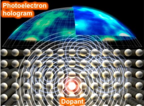 |
| Soft X-rays excite the core level electrons, leading to the emission of photoelectrons from various atoms, whose waves are then scattered by the surrounding atoms. The interference pattern between the scattered and direct photoelectron waves creates the photoelectron hologram, which may then be captured with an electron analyzer. CREDIT Nano Letters |
Abstract:
Scientists at Tokyo Institute of Technology (Tokyo Tech) and their research team involving researchers of JASRI, Osaka University, Nagoya Institute of Technology, and Nara Institute of Science and Technology have just developed a novel approach to determine and visualize the three-dimensional (3D) structure of individual dopant atoms using SPring-8. The technique will help improve the current understanding of the atomic structures of dopants in semiconductors correlated with their electrical activity and thus help support the development of new manufacturing processes for high-performance devices.
Viewing atomic structures of dopant atoms in 3-D relating to electrical activity in a semiconductor
Tokyo, Japan | Posted on December 28th, 2017Using a combination of spectro-photoelectron holography, electrical property measurements, and first-principles dynamics simulations, the 3D atomic structures of dopant impurities in a semiconductor crystal were successfully revealed. The need for a better understanding of the atomic structures of dopants in semiconductors had been long felt, mainly because the current limitations on active dopant concentrations result from the deactivation of excess dopant atoms by the formation of various types of clusters and other defect structures.
The search for techniques to electrically activate the dopant impurities in semiconductors with high efficiency and/or at high concentrations have always been an essential aspect of semiconductor device technology. However, despite various successful developments, the achievable maximum concentration of active dopants remains limited. Given the impact of the dopant atomic structures in this process, these structures had been previously investigated using both theoretical and experimental approaches. However, direct observation of the 3D structures of the dopant atomic arrangements had hitherto been difficult to achieve.
In this study, Kazuo Tsutsui at Tokyo Tech and colleagues involving researchers at JASRI, Osaka University, Nagoya Institute of Technology, and Nara Institute of Science and Technology developed spectro-photoelectron holography using SPring-8, and leveraged the capabilities of photoelectron holography in determining the concentrations of dopants at different sites, based on the peak intensities of the photoelectron spectrum, and classified electrically active / inactive atomic sites. These structures directly related with the density of carriers. In this approach, soft X-ray excitation of the core level electrons leads to the emission of photoelectrons from various atoms, whose waves are then scattered by the surrounding atoms. The resulting interference pattern creates the photoelectron hologram, which may then be captured with an electron analyzer. The photoelectron spectra acquired in this manner contain information from more than one atomic site. Therefore, peak fitting is performed to obtain the photoelectron hologram of individual atomic sites. The combination of this technique with first-principles simulations allows the successful estimation of the 3D structure of the dopant atoms, and the assessment of their different chemical bonding states. The method was used to estimate the 3D structures of arsenic atoms doped onto a silicon surface. The obtained results fully demonstrated the power of the proposed method and allowed confirmation of several previous results.
This work demonstrates the potential of spectro-photoelectron holography for the analysis of impurities in semiconductors. This technique allows analyses that are difficult to perform with conventional approaches and should therefore be useful in the development of improved doping techniques and, ultimately, in supporting the manufacture of high-performance devices.
####
About Tokyo Institute of Technology
Tokyo Institute of Technology stands at the forefront of research and higher education as the leading university for science and technology in Japan. Tokyo Tech researchers excel in a variety of fields, such as material science, biology, computer science and physics. Founded in 1881, Tokyo Tech has grown to host 10,000 undergraduate and graduate students who become principled leaders of their fields and some of the most sought-after scientists and engineers at top companies. Embodying the Japanese philosophy of "monotsukuri," meaning technical ingenuity and innovation, the Tokyo Tech community strives to make significant contributions to society through high-impact research.
Website: http://www.titech.ac.jp/english/
SPring-8
The name "SPring-8" comes from "Super Photon ring-8 GeV". It is owned by RIKEN and located in Harima Science Garden City, Hyogo Prefecture, Japan. SPring-8 generates the world's highest-performance synchrotron radiation and was opened in 1997 to users from universities, research institutes, and companies. Synchrotron radiation is an electromagnetic wave that is produced when electron beams, accelerated to nearly the speed of light, are bent in a high magnetic field. High-intensity synchrotron radiation in a wide range of energy from infrared to soft and hard X-ray regions is available at SPring-8.
About Osaka University
Osaka University was founded in 1931 as one of the seven imperial universities of Japan and now has expanded to one of Japan's leading comprehensive universities.?The University has now embarked on open research revolution from a position as Japan's most innovative university and among the most innovative institutions in the world according to Reuters 2015 Top 100 Innovative Universities and the Nature Index Innovation 2017. The university's ability to innovate from the stage of fundamental research through the creation of useful technology with economic impact stems from its broad disciplinary spectrum.
Website: http://resou.osaka-u.ac.jp/en/top
About NAIST
NAIST was founded in 1991 as a Japanese national university consisting solely of graduate schools in three integrated areas: information science, biological sciences, and materials science. In the early 2018, NAIST will transform its current structure into the one graduate school system to further promote the mission of cultivating global leaders in science and technology who will actively respond to social demands. At present, about 1,000 students -22% from overseas- are supervised by roughly 200 NAIST faculty. With its cutting-edge facilities and a 5 to 1 student-to-faculty ratio, NAIST's world-leading research and education are a direct result of its rich, global environment and supportive infrastructure. NAIST has quickly established itself as a world-class research and education center where young scientists and technologists become tomorrow's global leaders. For more detail please visit: http://www.naist.jp/en/
For more information, please click here
Contacts:
Emiko Kawaguchi
81-357-342-975
Copyright © Tokyo Institute of Technology
If you have a comment, please Contact us.Issuers of news releases, not 7th Wave, Inc. or Nanotechnology Now, are solely responsible for the accuracy of the content.
Bookmark:


| Related Links |
| Related News Press |
News and information
![]() Quantum computer improves AI predictions April 17th, 2026
Quantum computer improves AI predictions April 17th, 2026
![]() Flexible sensor gains sensitivity under pressure April 17th, 2026
Flexible sensor gains sensitivity under pressure April 17th, 2026
![]() A reusable chip for particulate matter sensing April 17th, 2026
A reusable chip for particulate matter sensing April 17th, 2026
![]() Detecting vibrational quantum beating in the predissociation dynamics of SF6 using time-resolved photoelectron spectroscopy April 17th, 2026
Detecting vibrational quantum beating in the predissociation dynamics of SF6 using time-resolved photoelectron spectroscopy April 17th, 2026
Imaging
![]() Simple algorithm paired with standard imaging tool could predict failure in lithium metal batteries August 8th, 2025
Simple algorithm paired with standard imaging tool could predict failure in lithium metal batteries August 8th, 2025
Possible Futures
![]() A fundamentally new therapeutic approach to cystic fibrosis: Nanobody repairs cellular defect April 17th, 2026
A fundamentally new therapeutic approach to cystic fibrosis: Nanobody repairs cellular defect April 17th, 2026
![]() UC Irvine physicists discover method to reverse �quantum scrambling� : The work addresses the problem of information loss in quantum computing system April 17th, 2026
UC Irvine physicists discover method to reverse �quantum scrambling� : The work addresses the problem of information loss in quantum computing system April 17th, 2026
Chip Technology
![]() A reusable chip for particulate matter sensing April 17th, 2026
A reusable chip for particulate matter sensing April 17th, 2026
![]() Metasurfaces smooth light to boost magnetic sensing precision January 30th, 2026
Metasurfaces smooth light to boost magnetic sensing precision January 30th, 2026
Nanoelectronics
![]() Lab to industry: InSe wafer-scale breakthrough for future electronics August 8th, 2025
Lab to industry: InSe wafer-scale breakthrough for future electronics August 8th, 2025
![]() Interdisciplinary: Rice team tackles the future of semiconductors Multiferroics could be the key to ultralow-energy computing October 6th, 2023
Interdisciplinary: Rice team tackles the future of semiconductors Multiferroics could be the key to ultralow-energy computing October 6th, 2023
![]() Key element for a scalable quantum computer: Physicists from Forschungszentrum J�lich and RWTH Aachen University demonstrate electron transport on a quantum chip September 23rd, 2022
Key element for a scalable quantum computer: Physicists from Forschungszentrum J�lich and RWTH Aachen University demonstrate electron transport on a quantum chip September 23rd, 2022
![]() Reduced power consumption in semiconductor devices September 23rd, 2022
Reduced power consumption in semiconductor devices September 23rd, 2022
Discoveries
![]() Quantum computer improves AI predictions April 17th, 2026
Quantum computer improves AI predictions April 17th, 2026
![]() Flexible sensor gains sensitivity under pressure April 17th, 2026
Flexible sensor gains sensitivity under pressure April 17th, 2026
![]() A reusable chip for particulate matter sensing April 17th, 2026
A reusable chip for particulate matter sensing April 17th, 2026
![]() Detecting vibrational quantum beating in the predissociation dynamics of SF6 using time-resolved photoelectron spectroscopy April 17th, 2026
Detecting vibrational quantum beating in the predissociation dynamics of SF6 using time-resolved photoelectron spectroscopy April 17th, 2026
Announcements
![]() A fundamentally new therapeutic approach to cystic fibrosis: Nanobody repairs cellular defect April 17th, 2026
A fundamentally new therapeutic approach to cystic fibrosis: Nanobody repairs cellular defect April 17th, 2026
![]() UC Irvine physicists discover method to reverse �quantum scrambling� : The work addresses the problem of information loss in quantum computing system April 17th, 2026
UC Irvine physicists discover method to reverse �quantum scrambling� : The work addresses the problem of information loss in quantum computing system April 17th, 2026
Interviews/Book Reviews/Essays/Reports/Podcasts/Journals/White papers/Posters
![]() A fundamentally new therapeutic approach to cystic fibrosis: Nanobody repairs cellular defect April 17th, 2026
A fundamentally new therapeutic approach to cystic fibrosis: Nanobody repairs cellular defect April 17th, 2026
![]() UC Irvine physicists discover method to reverse �quantum scrambling� : The work addresses the problem of information loss in quantum computing system April 17th, 2026
UC Irvine physicists discover method to reverse �quantum scrambling� : The work addresses the problem of information loss in quantum computing system April 17th, 2026
Tools
![]() Metasurfaces smooth light to boost magnetic sensing precision January 30th, 2026
Metasurfaces smooth light to boost magnetic sensing precision January 30th, 2026
![]() From sensors to smart systems: the rise of AI-driven photonic noses January 30th, 2026
From sensors to smart systems: the rise of AI-driven photonic noses January 30th, 2026
![]() Japan launches fully domestically produced quantum computer: Expo visitors to experience quantum computing firsthand August 8th, 2025
Japan launches fully domestically produced quantum computer: Expo visitors to experience quantum computing firsthand August 8th, 2025
|
|
||
|
|
||
| The latest news from around the world, FREE | ||
|
|
||
|
|
||
| Premium Products | ||
|
|
||
|
Only the news you want to read!
Learn More |
||
|
|
||
|
Full-service, expert consulting
Learn More |
||
|
|
||