Home > Press > MIPT scientists revisit optical constants of ultrathin gold films
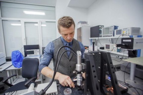 |
| Valentyn Volkov, the principal investigator, is the head of the Laboratory of Nanooptics and Plasmonics at MIPT. CREDIT MIPT |
Abstract:
Researchers at MIPT have conducted highly precise measurements of the optical constants of ultrathin gold films with thicknesses ranging from 20 to 200 billionths of a meter in the optical part of the electromagnetic spectrum. Thin gold films are key components of modern micro- and nanoscale optical and optoelectronic devices. The research findings will be in demand among researchers in the field. The paper was published in the journal Optics Express.
MIPT scientists revisit optical constants of ultrathin gold films
Moscow, Russia | Posted on October 20th, 2017Metal films with a thickness of tens of nanometers, or tens of billionths of a meter, are widely used to produce compact chemical and biological sensors, photodetectors, solar cells, and components for optical computers. When nanofilms are made thinner than 10 nanometers, they become not just conductive but also flexible and transparent, which might be applicable in a variety of modern devices.
Gold, which is widely used in nanoscale device development, has proved to be the most suitable metal for the purpose. Such applications require gold in the form of very thin films or nanostructures. To develop and optimize devices, precise data on the properties of such films are necessary. But most of the data used by researchers at present are reported in papers published almost half a century ago. For instance, one of the most frequently cited articles on the optical constants of gold is "Optical constants of the noble metals" by P.B. Johnson and R.W. Christy, published as early as 1972. The Scopus citation database reveals that the reference constants for gold from this paper have been used in at least 10,000 other publications. To appreciate the significance of this work, it is important to keep in mind that in the 70s, research into the optical properties of thin metal films required a tremendous effort, because the challenging experiments had to be followed by complex calculations and computers were not yet widespread.
Thinner is better
State-of-the-art laboratory equipment and the nearly unlimited computing power available to modern researchers enable more detailed studies of thin metal films. However, it is known that the optical properties of such films -- and therefore the efficiency of devices based on them -- depend on factors such as film thickness, deposition rate, and the temperature of the substrate used for film deposition. Accordingly, the MIPT researchers adjusted the initial conditions, namely the deposition rate and the substrate temperature, so as to optimize the optical properties of the film. After that, they conducted the necessary measurements by means of spectroscopic ellipsometry, X-ray diffractometry, electron and atomic force microscopy. The data obtained allowed the MIPT team to study in detail how the properties of thin gold films are related to their structure and average grain size.
The structure of a material affects its physical properties to a large extent, because it is at grain boundaries that conduction electrons are scattered, losing energy -- the way a ball in a pinball machine loses its momentum as it runs into obstacles. As it turned out, both optical losses and direct current resistivity are substantially increased, as the thickness of the gold film is reduced to below 80 nanometers. The authors of the paper provide reference data on the optical constants of gold for a wide range of wavelengths, from 300 to 2,000 nanometers, for films that are 20 to 200 nanometers thick. These findings will be of use to researchers working on various nanophotonic devices and metamaterials.
State-of-the-art technology
To grow thin films, the researchers used a technique called electron beam evaporation, which involves the following steps:: A purified silicon substrate is introduced into a vacuum chamber. Opposite the substrate, a metal sample is positioned. The metal, in this case gold, is then subjected to a beam of electrons accelerated by an electric field. This rapidly heats up the gold causing it to melt and eventually transform into vapor. The evaporated gold atoms are then transported across a region of low pressure from their source and undergo condensation on the substrate to form the thin film.
"Provided that you maintain a high vacuum, heat the metal appropriately, and otherwise follow the procedure, this technique yields films of arbitrary thickness, which is determined by the evaporation time. Moreover, the films are almost perfectly smooth, having a roughness of less than a nanometer," comments Valentyn Volkov, who heads the Laboratory of Nanooptics and Plasmonics at MIPT. "Such films can be used in optics and optoelectronics to develop high-sensitivity compact biosensors, solar cells, broadband photodetectors, and optoelectronic computer components." Gold films of this kind with a thickness of about 40 nanometers are already used in biosensor design.
####
For more information, please click here
Contacts:
Ilyana Zolotareva
7-977-771-4699
Copyright © Moscow Institute of Physics and Technology
If you have a comment, please Contact us.Issuers of news releases, not 7th Wave, Inc. or Nanotechnology Now, are solely responsible for the accuracy of the content.
Bookmark:


| Related Links |
| Related News Press |
News and information
![]() Quantum computer improves AI predictions April 17th, 2026
Quantum computer improves AI predictions April 17th, 2026
![]() Flexible sensor gains sensitivity under pressure April 17th, 2026
Flexible sensor gains sensitivity under pressure April 17th, 2026
![]() A reusable chip for particulate matter sensing April 17th, 2026
A reusable chip for particulate matter sensing April 17th, 2026
![]() Detecting vibrational quantum beating in the predissociation dynamics of SF6 using time-resolved photoelectron spectroscopy April 17th, 2026
Detecting vibrational quantum beating in the predissociation dynamics of SF6 using time-resolved photoelectron spectroscopy April 17th, 2026
Thin films
![]() Tiny nanosheets, big leap: A new sensor detects ethanol at ultra-low levels January 30th, 2026
Tiny nanosheets, big leap: A new sensor detects ethanol at ultra-low levels January 30th, 2026
![]() Utilizing palladium for addressing contact issues of buried oxide thin film transistors April 5th, 2024
Utilizing palladium for addressing contact issues of buried oxide thin film transistors April 5th, 2024
![]() Understanding the mechanism of non-uniform formation of diamond film on tools: Paving the way to a dry process with less environmental impact March 24th, 2023
Understanding the mechanism of non-uniform formation of diamond film on tools: Paving the way to a dry process with less environmental impact March 24th, 2023
![]() New study introduces the best graphite films: The work by Distinguished Professor Feng Ding at UNIST has been published in the October 2022 issue of Nature Nanotechnology November 4th, 2022
New study introduces the best graphite films: The work by Distinguished Professor Feng Ding at UNIST has been published in the October 2022 issue of Nature Nanotechnology November 4th, 2022
Chip Technology
![]() A reusable chip for particulate matter sensing April 17th, 2026
A reusable chip for particulate matter sensing April 17th, 2026
![]() Metasurfaces smooth light to boost magnetic sensing precision January 30th, 2026
Metasurfaces smooth light to boost magnetic sensing precision January 30th, 2026
Optical computing/Photonic computing
![]() ICFO researchers overcome long-standing bottleneck in single photon detection with twisted 2D materials August 8th, 2025
ICFO researchers overcome long-standing bottleneck in single photon detection with twisted 2D materials August 8th, 2025
![]() Programmable electron-induced color router array May 14th, 2025
Programmable electron-induced color router array May 14th, 2025
Sensors
![]() Flexible sensor gains sensitivity under pressure April 17th, 2026
Flexible sensor gains sensitivity under pressure April 17th, 2026
![]() Tiny nanosheets, big leap: A new sensor detects ethanol at ultra-low levels January 30th, 2026
Tiny nanosheets, big leap: A new sensor detects ethanol at ultra-low levels January 30th, 2026
![]() From sensors to smart systems: the rise of AI-driven photonic noses January 30th, 2026
From sensors to smart systems: the rise of AI-driven photonic noses January 30th, 2026
![]() Sensors innovations for smart lithium-based batteries: advancements, opportunities, and potential challenges August 8th, 2025
Sensors innovations for smart lithium-based batteries: advancements, opportunities, and potential challenges August 8th, 2025
Discoveries
![]() Quantum computer improves AI predictions April 17th, 2026
Quantum computer improves AI predictions April 17th, 2026
![]() Flexible sensor gains sensitivity under pressure April 17th, 2026
Flexible sensor gains sensitivity under pressure April 17th, 2026
![]() A reusable chip for particulate matter sensing April 17th, 2026
A reusable chip for particulate matter sensing April 17th, 2026
![]() Detecting vibrational quantum beating in the predissociation dynamics of SF6 using time-resolved photoelectron spectroscopy April 17th, 2026
Detecting vibrational quantum beating in the predissociation dynamics of SF6 using time-resolved photoelectron spectroscopy April 17th, 2026
Materials/Metamaterials/Magnetoresistance
![]() First real-time observation of two-dimensional melting process: Researchers at Mainz University unveil new insights into magnetic vortex structures August 8th, 2025
First real-time observation of two-dimensional melting process: Researchers at Mainz University unveil new insights into magnetic vortex structures August 8th, 2025
![]() Researchers unveil a groundbreaking clay-based solution to capture carbon dioxide and combat climate change June 6th, 2025
Researchers unveil a groundbreaking clay-based solution to capture carbon dioxide and combat climate change June 6th, 2025
![]() A 1960s idea inspires NBI researchers to study hitherto inaccessible quantum states June 6th, 2025
A 1960s idea inspires NBI researchers to study hitherto inaccessible quantum states June 6th, 2025
![]() Institute for Nanoscience hosts annual proposal planning meeting May 16th, 2025
Institute for Nanoscience hosts annual proposal planning meeting May 16th, 2025
Announcements
![]() A fundamentally new therapeutic approach to cystic fibrosis: Nanobody repairs cellular defect April 17th, 2026
A fundamentally new therapeutic approach to cystic fibrosis: Nanobody repairs cellular defect April 17th, 2026
![]() UC Irvine physicists discover method to reverse �quantum scrambling� : The work addresses the problem of information loss in quantum computing system April 17th, 2026
UC Irvine physicists discover method to reverse �quantum scrambling� : The work addresses the problem of information loss in quantum computing system April 17th, 2026
Interviews/Book Reviews/Essays/Reports/Podcasts/Journals/White papers/Posters
![]() A fundamentally new therapeutic approach to cystic fibrosis: Nanobody repairs cellular defect April 17th, 2026
A fundamentally new therapeutic approach to cystic fibrosis: Nanobody repairs cellular defect April 17th, 2026
![]() UC Irvine physicists discover method to reverse �quantum scrambling� : The work addresses the problem of information loss in quantum computing system April 17th, 2026
UC Irvine physicists discover method to reverse �quantum scrambling� : The work addresses the problem of information loss in quantum computing system April 17th, 2026
Photonics/Optics/Lasers
![]() Metasurfaces smooth light to boost magnetic sensing precision January 30th, 2026
Metasurfaces smooth light to boost magnetic sensing precision January 30th, 2026
![]() From sensors to smart systems: the rise of AI-driven photonic noses January 30th, 2026
From sensors to smart systems: the rise of AI-driven photonic noses January 30th, 2026
|
|
||
|
|
||
| The latest news from around the world, FREE | ||
|
|
||
|
|
||
| Premium Products | ||
|
|
||
|
Only the news you want to read!
Learn More |
||
|
|
||
|
Full-service, expert consulting
Learn More |
||
|
|
||