Home > Press > Injecting electrons jolts 2-D structure into new atomic pattern: Berkeley Lab study is first to show potential of energy-efficient next-gen electronic memory
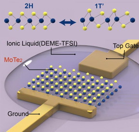 |
| Schematic shows the configuration for structural phase transition on a molybdenum ditelluride monolayer (MoTe2, shown as yellow and blue spheres), which is anchored by a metal electrodes (top gate and ground). The ionic liquid covering the monolayer and electrodes enables a high density of electrons to populate the monolayer, leading to changes in the structural lattice from a hexagonal (2H) to monoclinic (1T') pattern. CREDIT Ying Wang/Berkeley Lab |
Abstract:
The same electrostatic charge that can make hair stand on end and attach balloons to clothing could be an efficient way to drive atomically thin electronic memory devices of the future, according to a new study led by researchers at the Department of Energy's Lawrence Berkeley National Laboratory (Berkeley Lab).
Injecting electrons jolts 2-D structure into new atomic pattern: Berkeley Lab study is first to show potential of energy-efficient next-gen electronic memory
Berkeley, CA | Posted on October 13th, 2017In a study published today in the journal Nature, scientists have found a way to reversibly change the atomic structure of a 2-D material by injecting, or "doping," it with electrons. The process uses far less energy than current methods for changing the configuration of a material's structure.
"We show, for the first time, that it is possible to inject electrons to drive structural phase changes in materials," said study principal investigator Xiang Zhang, senior faculty scientist at Berkeley Lab's Materials Sciences Division and a professor at UC Berkeley. "By adding electrons into a material, the overall energy goes up and will tip off the balance, resulting in the atomic structure re-arranging to a new pattern that is more stable. Such electron doping-driven structural phase transitions at the 2-D limit is not only important in fundamental physics; it also opens the door for new electronic memory and low-power switching in the next generation of ultra-thin devices."
Switching a material's structural configuration from one phase to another is the fundamental, binary characteristic that underlies today's digital circuitry. Electronic components capable of this phase transition have shrunk down to paper-thin sizes, but they are still considered to be bulk, 3-D layers by scientists. By comparison, 2-D monolayer materials are composed of a single layer of atoms or molecules whose thickness is 100,000 times as small as a human hair.
"The idea of electron doping to alter a material's atomic structure is unique to 2-D materials, which are much more electrically tunable compared with 3-D bulk materials," said study co-lead author Jun Xiao, a graduate student in Zhang's lab.
The classic approach to driving the structural transition of materials involves heating to above 500 degrees Celsius. Such methods are energy-intensive and not feasible for practical applications. In addition, the excess heat can significantly reduce the life span of components in integrated circuits.
A number of research groups have also investigated the use of chemicals to alter the configuration of atoms in semiconductor materials, but that process is still difficult to control and has not been widely adopted by industry.
"Here we use electrostatic doping to control the atomic configuration of a two-dimensional material," said study co-lead author Ying Wang, another graduate student in Zhang's lab. "Compared to the use of chemicals, our method is reversible and free of impurities. It has greater potential for integration into the manufacturing of cell phones, computers and other electronic devices."
The researchers used molybdenum ditelluride (MoTe2), a typical 2-D semiconductor, and coated it with an ionic liquid (DEME-TFSI), which has an ultra-high capacitance, or ability to store electric charges. The layer of ionic liquid allowed the researchers to inject the semiconductor with electrons at a density of a hundred trillion to a quadrillion per square centimeter. It is an electron density that is one to two orders higher in magnitude than what could be achieved in 3-D bulk materials, the researchers said.
Through spectroscopic analysis, the researchers determined that the injection of electrons changed the atoms' arrangement of the molybdenum ditelluride from a hexagonal shape to one that is monoclinic, which has more of a slanted cuboid shape. Once the electrons were retracted, the crystal structure returned to its original hexagonal pattern, showing that the phase transition is reversible. Moreover, these two types of atom arrangements have very different symmetries, providing a large contrast for applications in optical components.
"Such an atomically thin device could have dual functions, serving simultaneously as optical or electrical transistors, and hence broaden the functionalities of the electronics used in our daily lives," said Wang.
###
This work was supported by DOE's Office of Science and by the National Science Foundation.
####
About Lawrence Berkeley National Laboratory
Lawrence Berkeley National Laboratory addresses the world's most urgent scientific challenges by advancing sustainable energy, protecting human health, creating new materials, and revealing the origin and fate of the universe. Founded in 1931, Berkeley Lab's scientific expertise has been recognized with 13 Nobel Prizes. The University of California manages Berkeley Lab for the U.S. Department of Energy's Office of Science. For more, visit http://www.lbl.gov .
DOE's Office of Science is the single largest supporter of basic research in the physical sciences in the United States, and is working to address some of the most pressing challenges of our time. For more information, please visit science.energy.gov.
For more information, please click here
Contacts:
Sarah Yang
510-486-4575
Copyright © Lawrence Berkeley National Laboratory
If you have a comment, please Contact us.Issuers of news releases, not 7th Wave, Inc. or Nanotechnology Now, are solely responsible for the accuracy of the content.
Bookmark:


| Related Links |
| Related News Press |
News and information
![]() Quantum computer improves AI predictions April 17th, 2026
Quantum computer improves AI predictions April 17th, 2026
![]() Flexible sensor gains sensitivity under pressure April 17th, 2026
Flexible sensor gains sensitivity under pressure April 17th, 2026
![]() A reusable chip for particulate matter sensing April 17th, 2026
A reusable chip for particulate matter sensing April 17th, 2026
![]() Detecting vibrational quantum beating in the predissociation dynamics of SF6 using time-resolved photoelectron spectroscopy April 17th, 2026
Detecting vibrational quantum beating in the predissociation dynamics of SF6 using time-resolved photoelectron spectroscopy April 17th, 2026
2 Dimensional Materials
![]() Flexible sensor gains sensitivity under pressure April 17th, 2026
Flexible sensor gains sensitivity under pressure April 17th, 2026
![]() ICFO researchers overcome long-standing bottleneck in single photon detection with twisted 2D materials August 8th, 2025
ICFO researchers overcome long-standing bottleneck in single photon detection with twisted 2D materials August 8th, 2025
![]() First real-time observation of two-dimensional melting process: Researchers at Mainz University unveil new insights into magnetic vortex structures August 8th, 2025
First real-time observation of two-dimensional melting process: Researchers at Mainz University unveil new insights into magnetic vortex structures August 8th, 2025
![]() Lab to industry: InSe wafer-scale breakthrough for future electronics August 8th, 2025
Lab to industry: InSe wafer-scale breakthrough for future electronics August 8th, 2025
Laboratories
![]() Researchers develop molecular qubits that communicate at telecom frequencies October 3rd, 2025
Researchers develop molecular qubits that communicate at telecom frequencies October 3rd, 2025
Govt.-Legislation/Regulation/Funding/Policy
![]() Quantum computer improves AI predictions April 17th, 2026
Quantum computer improves AI predictions April 17th, 2026
![]() Metasurfaces smooth light to boost magnetic sensing precision January 30th, 2026
Metasurfaces smooth light to boost magnetic sensing precision January 30th, 2026
![]() New imaging approach transforms study of bacterial biofilms August 8th, 2025
New imaging approach transforms study of bacterial biofilms August 8th, 2025
Possible Futures
![]() A fundamentally new therapeutic approach to cystic fibrosis: Nanobody repairs cellular defect April 17th, 2026
A fundamentally new therapeutic approach to cystic fibrosis: Nanobody repairs cellular defect April 17th, 2026
![]() UC Irvine physicists discover method to reverse �quantum scrambling� : The work addresses the problem of information loss in quantum computing system April 17th, 2026
UC Irvine physicists discover method to reverse �quantum scrambling� : The work addresses the problem of information loss in quantum computing system April 17th, 2026
Chip Technology
![]() A reusable chip for particulate matter sensing April 17th, 2026
A reusable chip for particulate matter sensing April 17th, 2026
![]() Metasurfaces smooth light to boost magnetic sensing precision January 30th, 2026
Metasurfaces smooth light to boost magnetic sensing precision January 30th, 2026
Memory Technology
![]() Researchers tackle the memory bottleneck stalling quantum computing October 3rd, 2025
Researchers tackle the memory bottleneck stalling quantum computing October 3rd, 2025
![]() First real-time observation of two-dimensional melting process: Researchers at Mainz University unveil new insights into magnetic vortex structures August 8th, 2025
First real-time observation of two-dimensional melting process: Researchers at Mainz University unveil new insights into magnetic vortex structures August 8th, 2025
![]() Utilizing palladium for addressing contact issues of buried oxide thin film transistors April 5th, 2024
Utilizing palladium for addressing contact issues of buried oxide thin film transistors April 5th, 2024
Optical computing/Photonic computing
![]() ICFO researchers overcome long-standing bottleneck in single photon detection with twisted 2D materials August 8th, 2025
ICFO researchers overcome long-standing bottleneck in single photon detection with twisted 2D materials August 8th, 2025
![]() Programmable electron-induced color router array May 14th, 2025
Programmable electron-induced color router array May 14th, 2025
Discoveries
![]() Quantum computer improves AI predictions April 17th, 2026
Quantum computer improves AI predictions April 17th, 2026
![]() Flexible sensor gains sensitivity under pressure April 17th, 2026
Flexible sensor gains sensitivity under pressure April 17th, 2026
![]() A reusable chip for particulate matter sensing April 17th, 2026
A reusable chip for particulate matter sensing April 17th, 2026
![]() Detecting vibrational quantum beating in the predissociation dynamics of SF6 using time-resolved photoelectron spectroscopy April 17th, 2026
Detecting vibrational quantum beating in the predissociation dynamics of SF6 using time-resolved photoelectron spectroscopy April 17th, 2026
Materials/Metamaterials/Magnetoresistance
![]() First real-time observation of two-dimensional melting process: Researchers at Mainz University unveil new insights into magnetic vortex structures August 8th, 2025
First real-time observation of two-dimensional melting process: Researchers at Mainz University unveil new insights into magnetic vortex structures August 8th, 2025
![]() Researchers unveil a groundbreaking clay-based solution to capture carbon dioxide and combat climate change June 6th, 2025
Researchers unveil a groundbreaking clay-based solution to capture carbon dioxide and combat climate change June 6th, 2025
![]() A 1960s idea inspires NBI researchers to study hitherto inaccessible quantum states June 6th, 2025
A 1960s idea inspires NBI researchers to study hitherto inaccessible quantum states June 6th, 2025
![]() Institute for Nanoscience hosts annual proposal planning meeting May 16th, 2025
Institute for Nanoscience hosts annual proposal planning meeting May 16th, 2025
Announcements
![]() A fundamentally new therapeutic approach to cystic fibrosis: Nanobody repairs cellular defect April 17th, 2026
A fundamentally new therapeutic approach to cystic fibrosis: Nanobody repairs cellular defect April 17th, 2026
![]() UC Irvine physicists discover method to reverse �quantum scrambling� : The work addresses the problem of information loss in quantum computing system April 17th, 2026
UC Irvine physicists discover method to reverse �quantum scrambling� : The work addresses the problem of information loss in quantum computing system April 17th, 2026
Interviews/Book Reviews/Essays/Reports/Podcasts/Journals/White papers/Posters
![]() A fundamentally new therapeutic approach to cystic fibrosis: Nanobody repairs cellular defect April 17th, 2026
A fundamentally new therapeutic approach to cystic fibrosis: Nanobody repairs cellular defect April 17th, 2026
![]() UC Irvine physicists discover method to reverse �quantum scrambling� : The work addresses the problem of information loss in quantum computing system April 17th, 2026
UC Irvine physicists discover method to reverse �quantum scrambling� : The work addresses the problem of information loss in quantum computing system April 17th, 2026
Industrial
![]() Tiny nanosheets, big leap: A new sensor detects ethanol at ultra-low levels January 30th, 2026
Tiny nanosheets, big leap: A new sensor detects ethanol at ultra-low levels January 30th, 2026
![]() Quantum interference in molecule-surface collisions February 28th, 2025
Quantum interference in molecule-surface collisions February 28th, 2025
![]() Boron nitride nanotube fibers get real: Rice lab creates first heat-tolerant, stable fibers from wet-spinning process June 24th, 2022
Boron nitride nanotube fibers get real: Rice lab creates first heat-tolerant, stable fibers from wet-spinning process June 24th, 2022
Photonics/Optics/Lasers
![]() Metasurfaces smooth light to boost magnetic sensing precision January 30th, 2026
Metasurfaces smooth light to boost magnetic sensing precision January 30th, 2026
![]() From sensors to smart systems: the rise of AI-driven photonic noses January 30th, 2026
From sensors to smart systems: the rise of AI-driven photonic noses January 30th, 2026
|
|
||
|
|
||
| The latest news from around the world, FREE | ||
|
|
||
|
|
||
| Premium Products | ||
|
|
||
|
Only the news you want to read!
Learn More |
||
|
|
||
|
Full-service, expert consulting
Learn More |
||
|
|
||