Home > Press > Two dimensional materials: Advanced molybdenum selenide near infrared phototransistors
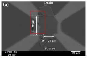 |
| Scanning electron microscopy image of the near-infrared photodetector based on few-layered MoSe2. |
Abstract:
Optical sensors operating in the near infrared (NIR) are important for applications in imaging, photodetectors, and biological sensors. Notably, recent reports on the synthesis of high quality, large areas of graphene has motivated researchers to search for other 2D materials with properties suitable for NIR devices.
Two dimensional materials: Advanced molybdenum selenide near infrared phototransistors
Tokyo, Japan | Posted on September 27th, 2017Now, Abdelkader Abderrahmane and colleagues at the University of Electro-Communications, Tokyo in collaboration with researchers at Chosun University, Korea, describe the optoelectronics characteristics of molybdenum selenide (MoSe2) phototransistors for applications to photodetectors. The application of gate voltages to the devices yielded a maximum photoresponsivity 238 A/W, an external quantum efficiency (EQE) of 37,745% under 785 nm light. The researchers state: "our device is one of the best high-performance nanoscale near-infrared photodetectors based on multilayered two-dimensional materials."
The devices were fabricated using few layered MoSe2 with a thickness of ~44 nm that was exfoliated from natural MoSe2 onto thermally oxidized silicon substrates with metallic strips acting as back gates. The transistor channel width and length were 50 and 20 μm, and the charge mobility was be 5.1 cm2 /V/s.
Electrical measurements indicated that the devices operated in the so-called accumulation mode and with a pinch off voltage of - 40V.
The combination of the 1.1 eV bandgap of MoSe2 and its high optical absorption compared to MoS2 is expected to offer wide ranging applications in optoelectronics.
####
About University of Electro-Communications
The University of Electro-Communications (UEC) in Tokyo is a small, luminous university at the forefront of pure and applied sciences, engineering, and technology research. Its roots go back to the Technical Institute for Wireless Commutations, which was established in 1918 by the Wireless Association to train so-called wireless engineers in maritime communications in response to the Titanic disaster in 1912. In 1949, the UEC was established as a national university by the Japanese Ministry of Education, and moved in 1957 from Meguro to its current Chofu campus Tokyo.
With approximately 4,000 students and 350 faculty, UEC is regarded as a small university, but with particular expertise in wireless communications, laser science, robotics, informatics, and material science, to name just a few areas of research.
The UEC was selected for the Ministry of Education, Culture, Sports, Science and Technology (MEXT) Program for Promoting the Enhancement of Research Universities as a result of its strengths in three main areas: optics and photonics research, where we are number one for the number of joint publications with foreign researchers; wireless communications, which reflects our roots; and materials-based research, particularly on fuel cells.
For more information, please click here
Contacts:
International Public Relations
The University of Electro-Communications, Tokyo
1-5-1 Chofugaoka, Chofu, Tokyo 182-8585
E-mail:
Website: http://www.uec.ac.jp/
Copyright © University of Electro-Communications
If you have a comment, please Contact us.Issuers of news releases, not 7th Wave, Inc. or Nanotechnology Now, are solely responsible for the accuracy of the content.
Bookmark:


| Related Links |
| Related News Press |
News and information
![]() Quantum computer improves AI predictions April 17th, 2026
Quantum computer improves AI predictions April 17th, 2026
![]() Flexible sensor gains sensitivity under pressure April 17th, 2026
Flexible sensor gains sensitivity under pressure April 17th, 2026
![]() A reusable chip for particulate matter sensing April 17th, 2026
A reusable chip for particulate matter sensing April 17th, 2026
![]() Detecting vibrational quantum beating in the predissociation dynamics of SF6 using time-resolved photoelectron spectroscopy April 17th, 2026
Detecting vibrational quantum beating in the predissociation dynamics of SF6 using time-resolved photoelectron spectroscopy April 17th, 2026
2 Dimensional Materials
![]() Flexible sensor gains sensitivity under pressure April 17th, 2026
Flexible sensor gains sensitivity under pressure April 17th, 2026
Possible Futures
![]() A fundamentally new therapeutic approach to cystic fibrosis: Nanobody repairs cellular defect April 17th, 2026
A fundamentally new therapeutic approach to cystic fibrosis: Nanobody repairs cellular defect April 17th, 2026
![]() UC Irvine physicists discover method to reverse �quantum scrambling� : The work addresses the problem of information loss in quantum computing system April 17th, 2026
UC Irvine physicists discover method to reverse �quantum scrambling� : The work addresses the problem of information loss in quantum computing system April 17th, 2026
Sensors
![]() Flexible sensor gains sensitivity under pressure April 17th, 2026
Flexible sensor gains sensitivity under pressure April 17th, 2026
![]() Tiny nanosheets, big leap: A new sensor detects ethanol at ultra-low levels January 30th, 2026
Tiny nanosheets, big leap: A new sensor detects ethanol at ultra-low levels January 30th, 2026
![]() From sensors to smart systems: the rise of AI-driven photonic noses January 30th, 2026
From sensors to smart systems: the rise of AI-driven photonic noses January 30th, 2026
![]() Sensors innovations for smart lithium-based batteries: advancements, opportunities, and potential challenges August 8th, 2025
Sensors innovations for smart lithium-based batteries: advancements, opportunities, and potential challenges August 8th, 2025
Discoveries
![]() Quantum computer improves AI predictions April 17th, 2026
Quantum computer improves AI predictions April 17th, 2026
![]() Flexible sensor gains sensitivity under pressure April 17th, 2026
Flexible sensor gains sensitivity under pressure April 17th, 2026
![]() A reusable chip for particulate matter sensing April 17th, 2026
A reusable chip for particulate matter sensing April 17th, 2026
![]() Detecting vibrational quantum beating in the predissociation dynamics of SF6 using time-resolved photoelectron spectroscopy April 17th, 2026
Detecting vibrational quantum beating in the predissociation dynamics of SF6 using time-resolved photoelectron spectroscopy April 17th, 2026
Materials/Metamaterials/Magnetoresistance
![]() First real-time observation of two-dimensional melting process: Researchers at Mainz University unveil new insights into magnetic vortex structures August 8th, 2025
First real-time observation of two-dimensional melting process: Researchers at Mainz University unveil new insights into magnetic vortex structures August 8th, 2025
![]() Researchers unveil a groundbreaking clay-based solution to capture carbon dioxide and combat climate change June 6th, 2025
Researchers unveil a groundbreaking clay-based solution to capture carbon dioxide and combat climate change June 6th, 2025
![]() A 1960s idea inspires NBI researchers to study hitherto inaccessible quantum states June 6th, 2025
A 1960s idea inspires NBI researchers to study hitherto inaccessible quantum states June 6th, 2025
![]() Institute for Nanoscience hosts annual proposal planning meeting May 16th, 2025
Institute for Nanoscience hosts annual proposal planning meeting May 16th, 2025
Announcements
![]() A fundamentally new therapeutic approach to cystic fibrosis: Nanobody repairs cellular defect April 17th, 2026
A fundamentally new therapeutic approach to cystic fibrosis: Nanobody repairs cellular defect April 17th, 2026
![]() UC Irvine physicists discover method to reverse �quantum scrambling� : The work addresses the problem of information loss in quantum computing system April 17th, 2026
UC Irvine physicists discover method to reverse �quantum scrambling� : The work addresses the problem of information loss in quantum computing system April 17th, 2026
Interviews/Book Reviews/Essays/Reports/Podcasts/Journals/White papers/Posters
![]() A fundamentally new therapeutic approach to cystic fibrosis: Nanobody repairs cellular defect April 17th, 2026
A fundamentally new therapeutic approach to cystic fibrosis: Nanobody repairs cellular defect April 17th, 2026
![]() UC Irvine physicists discover method to reverse �quantum scrambling� : The work addresses the problem of information loss in quantum computing system April 17th, 2026
UC Irvine physicists discover method to reverse �quantum scrambling� : The work addresses the problem of information loss in quantum computing system April 17th, 2026
Photonics/Optics/Lasers
![]() Metasurfaces smooth light to boost magnetic sensing precision January 30th, 2026
Metasurfaces smooth light to boost magnetic sensing precision January 30th, 2026
![]() From sensors to smart systems: the rise of AI-driven photonic noses January 30th, 2026
From sensors to smart systems: the rise of AI-driven photonic noses January 30th, 2026
|
|
||
|
|
||
| The latest news from around the world, FREE | ||
|
|
||
|
|
||
| Premium Products | ||
|
|
||
|
Only the news you want to read!
Learn More |
||
|
|
||
|
Full-service, expert consulting
Learn More |
||
|
|
||