Home > Press > New results reveal high tunability of 2-D material: Berkeley Lab-led team also provides most precise band gap measurement yet for hotly studied monolayer moly sulfide
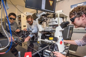 |
| From left: Kaiyuan Yao, Nick Borys, and P. James Schuck, seen here at Berkeley Lab's Molecular Foundry, measured a property in a 2-D material that could help realize new applications. CREDIT Marilyn Chung/Berkeley Lab |
Abstract:
Two-dimensional materials are a sort of a rookie phenom in the scientific community. They are atomically thin and can exhibit radically different electronic and light-based properties than their thicker, more conventional forms, so researchers are flocking to this fledgling field to find ways to tap these exotic traits.
New results reveal high tunability of 2-D material: Berkeley Lab-led team also provides most precise band gap measurement yet for hotly studied monolayer moly sulfide
Berkeley, CA | Posted on August 26th, 2017Applications for 2-D materials range from microchip components to superthin and flexible solar panels and display screens, among a growing list of possible uses. But because their fundamental structure is inherently tiny, they can be tricky to manufacture and measure, and to match with other materials. So while 2-D materials R&D is on the rise, there are still many unknowns about how to isolate, enhance, and manipulate their most desirable qualities.
Now, a science team at the Department of Energy's Lawrence Berkeley National Laboratory (Berkeley Lab) has precisely measured some previously obscured properties of moly sulfide, a 2-D semiconducting material also known as molybdenum disulfide or MoS2. The team also revealed a powerful tuning mechanism and an interrelationship between its electronic and optical, or light-related, properties.
To best incorporate such monolayer materials into electronic devices, engineers want to know the "band gap," which is the minimum energy level it takes to jolt electrons away from the atoms they are coupled to, so that they flow freely through the material as electric current flows through a copper wire. Supplying sufficient energy to the electrons by absorbing light, for example, converts the material into an electrically conducting state.
As reported in the Aug. 25 issue of Physical Review Letters, researchers measured the band gap for a monolayer of moly sulfide, which has proved difficult to accurately predict theoretically, and found it to be about 30 percent higher than expected based on previous experiments. They also quantified how the band gap changes with electron density - a phenomenon known as "band gap renormalization."
"The most critical significance of this work was in finding the band gap," said Kaiyuan Yao, a graduate student researcher at Berkeley Lab and the University of California, Berkeley, who served as the lead author of the research paper.
"That provides very important guidance to all of the optoelectronic device engineers. They need to know what the band gap is" in orderly to properly connect the 2-D material with other materials and components in a device, Yao said.
Obtaining the direct band gap measurement is challenged by the so-called "exciton effect" in 2-D materials that is produced by a strong pairing between electrons and electron "holes" �- vacant positions around an atom where an electron can exist. The strength of this effect can mask measurements of the band gap.
Nicholas Borys, a project scientist at Berkeley Lab's Molecular Foundry who also participated in the study, said the study also resolves how to tune optical and electronic properties in a 2-D material.
"The real power of our technique, and an important milestone for the physics community, is to discern between these optical and electronic properties," Borys said.
The team used several tools at the Molecular Foundry, a facility that is open to the scientific community and specializes in the creation and exploration of nanoscale materials.
The Molecular Foundry technique that researchers adapted for use in studying monolayer moly sulfide, known as photoluminescence excitation (PLE) spectroscopy, promises to bring new applications for the material within reach, such as ultrasensitive biosensors and tinier transistors, and also shows promise for similarly pinpointing and manipulating properties in other 2-D materials, researchers said.
The research team measured both the exciton and band gap signals, and then detangled these separate signals. Scientists observed how light was absorbed by electrons in the moly sulfide sample as they adjusted the density of electrons crammed into the sample by changing the electrical voltage on a layer of charged silicon that sat below the moly sulfide monolayer.
Researchers noticed a slight "bump" in their measurements that they realized was a direct measurement of the band gap, and through a slew of other experiments used their discovery to study how the band gap was readily tunable by simply adjusting the density of electrons in the material.
"The large degree of tunability really opens people's eyes," said P. James Schuck, who was director of the Imaging and Manipulation of Nanostructures facility at the Molecular Foundry during this study.
"And because we could see both the band gap's edge and the excitons simultaneously, we could understand each independently and also understand the relationship between them," said Schuck, now at Columbia University. "It turns out all of these properties are dependent on one another."
Moly sulfide, Schuck also noted, is "extremely sensitive to its local environment," which makes it a prime candidate for use in a range of sensors. Because it is highly sensitive to both optical and electronic effects, it could translate incoming light into electronic signals and vice versa.
Schuck said the team hopes to use a suite of techniques at the Molecular Foundry to create other types of monolayer materials and samples of stacked 2-D layers, and to obtain definitive band gap measurements for these, too. "It turns out no one yet knows the band gaps for some of these other materials," he said.
The team also has expertise in the use of a nanoscale probe to map the electronic behavior across a given sample.
Borys added, "We certainly hope this work seeds further studies on other 2-D semiconductor systems."
The Molecular Foundry is a DOE Office of Science User Facility that provides free access to state-of-the-art equipment and multidisciplinary expertise in nanoscale science to visiting scientists.
Researchers from the Kavli Energy NanoSciences Institute at UC Berkeley and Berkeley Lab, and from Arizona State University also participated in this study, which was supported by the National Science Foundation.
####
About Lawrence Berkeley National Laboratory
Lawrence Berkeley National Laboratory addresses the world's most urgent scientific challenges by advancing sustainable energy, protecting human health, creating new materials, and revealing the origin and fate of the universe. Founded in 1931, Berkeley Lab's scientific expertise has been recognized with 13 Nobel Prizes. The University of California manages Berkeley Lab for the U.S. Department of Energy's Office of Science. For more, visit http://www.lbl.gov.
DOE's Office of Science is the single largest supporter of basic research in the physical sciences in the United States, and is working to address some of the most pressing challenges of our time. For more information, please visit science.energy.gov.
For more information, please click here
Contacts:
Glenn Roberts Jr.
510-486-5582
Copyright © Lawrence Berkeley National Laboratory
If you have a comment, please Contact us.Issuers of news releases, not 7th Wave, Inc. or Nanotechnology Now, are solely responsible for the accuracy of the content.
Bookmark:


| Related Links |
| Related News Press |
News and information
![]() Quantum computer improves AI predictions April 17th, 2026
Quantum computer improves AI predictions April 17th, 2026
![]() Flexible sensor gains sensitivity under pressure April 17th, 2026
Flexible sensor gains sensitivity under pressure April 17th, 2026
![]() A reusable chip for particulate matter sensing April 17th, 2026
A reusable chip for particulate matter sensing April 17th, 2026
![]() Detecting vibrational quantum beating in the predissociation dynamics of SF6 using time-resolved photoelectron spectroscopy April 17th, 2026
Detecting vibrational quantum beating in the predissociation dynamics of SF6 using time-resolved photoelectron spectroscopy April 17th, 2026
2 Dimensional Materials
![]() Flexible sensor gains sensitivity under pressure April 17th, 2026
Flexible sensor gains sensitivity under pressure April 17th, 2026
![]() ICFO researchers overcome long-standing bottleneck in single photon detection with twisted 2D materials August 8th, 2025
ICFO researchers overcome long-standing bottleneck in single photon detection with twisted 2D materials August 8th, 2025
![]() First real-time observation of two-dimensional melting process: Researchers at Mainz University unveil new insights into magnetic vortex structures August 8th, 2025
First real-time observation of two-dimensional melting process: Researchers at Mainz University unveil new insights into magnetic vortex structures August 8th, 2025
![]() Lab to industry: InSe wafer-scale breakthrough for future electronics August 8th, 2025
Lab to industry: InSe wafer-scale breakthrough for future electronics August 8th, 2025
Laboratories
![]() Researchers develop molecular qubits that communicate at telecom frequencies October 3rd, 2025
Researchers develop molecular qubits that communicate at telecom frequencies October 3rd, 2025
Govt.-Legislation/Regulation/Funding/Policy
![]() Quantum computer improves AI predictions April 17th, 2026
Quantum computer improves AI predictions April 17th, 2026
![]() Metasurfaces smooth light to boost magnetic sensing precision January 30th, 2026
Metasurfaces smooth light to boost magnetic sensing precision January 30th, 2026
![]() New imaging approach transforms study of bacterial biofilms August 8th, 2025
New imaging approach transforms study of bacterial biofilms August 8th, 2025
Possible Futures
![]() A fundamentally new therapeutic approach to cystic fibrosis: Nanobody repairs cellular defect April 17th, 2026
A fundamentally new therapeutic approach to cystic fibrosis: Nanobody repairs cellular defect April 17th, 2026
![]() UC Irvine physicists discover method to reverse �quantum scrambling� : The work addresses the problem of information loss in quantum computing system April 17th, 2026
UC Irvine physicists discover method to reverse �quantum scrambling� : The work addresses the problem of information loss in quantum computing system April 17th, 2026
Chip Technology
![]() A reusable chip for particulate matter sensing April 17th, 2026
A reusable chip for particulate matter sensing April 17th, 2026
![]() Metasurfaces smooth light to boost magnetic sensing precision January 30th, 2026
Metasurfaces smooth light to boost magnetic sensing precision January 30th, 2026
Optical computing/Photonic computing
![]() ICFO researchers overcome long-standing bottleneck in single photon detection with twisted 2D materials August 8th, 2025
ICFO researchers overcome long-standing bottleneck in single photon detection with twisted 2D materials August 8th, 2025
![]() Programmable electron-induced color router array May 14th, 2025
Programmable electron-induced color router array May 14th, 2025
Sensors
![]() Flexible sensor gains sensitivity under pressure April 17th, 2026
Flexible sensor gains sensitivity under pressure April 17th, 2026
![]() Tiny nanosheets, big leap: A new sensor detects ethanol at ultra-low levels January 30th, 2026
Tiny nanosheets, big leap: A new sensor detects ethanol at ultra-low levels January 30th, 2026
![]() From sensors to smart systems: the rise of AI-driven photonic noses January 30th, 2026
From sensors to smart systems: the rise of AI-driven photonic noses January 30th, 2026
![]() Sensors innovations for smart lithium-based batteries: advancements, opportunities, and potential challenges August 8th, 2025
Sensors innovations for smart lithium-based batteries: advancements, opportunities, and potential challenges August 8th, 2025
Discoveries
![]() Quantum computer improves AI predictions April 17th, 2026
Quantum computer improves AI predictions April 17th, 2026
![]() Flexible sensor gains sensitivity under pressure April 17th, 2026
Flexible sensor gains sensitivity under pressure April 17th, 2026
![]() A reusable chip for particulate matter sensing April 17th, 2026
A reusable chip for particulate matter sensing April 17th, 2026
![]() Detecting vibrational quantum beating in the predissociation dynamics of SF6 using time-resolved photoelectron spectroscopy April 17th, 2026
Detecting vibrational quantum beating in the predissociation dynamics of SF6 using time-resolved photoelectron spectroscopy April 17th, 2026
Materials/Metamaterials/Magnetoresistance
![]() First real-time observation of two-dimensional melting process: Researchers at Mainz University unveil new insights into magnetic vortex structures August 8th, 2025
First real-time observation of two-dimensional melting process: Researchers at Mainz University unveil new insights into magnetic vortex structures August 8th, 2025
![]() Researchers unveil a groundbreaking clay-based solution to capture carbon dioxide and combat climate change June 6th, 2025
Researchers unveil a groundbreaking clay-based solution to capture carbon dioxide and combat climate change June 6th, 2025
![]() A 1960s idea inspires NBI researchers to study hitherto inaccessible quantum states June 6th, 2025
A 1960s idea inspires NBI researchers to study hitherto inaccessible quantum states June 6th, 2025
![]() Institute for Nanoscience hosts annual proposal planning meeting May 16th, 2025
Institute for Nanoscience hosts annual proposal planning meeting May 16th, 2025
Announcements
![]() A fundamentally new therapeutic approach to cystic fibrosis: Nanobody repairs cellular defect April 17th, 2026
A fundamentally new therapeutic approach to cystic fibrosis: Nanobody repairs cellular defect April 17th, 2026
![]() UC Irvine physicists discover method to reverse �quantum scrambling� : The work addresses the problem of information loss in quantum computing system April 17th, 2026
UC Irvine physicists discover method to reverse �quantum scrambling� : The work addresses the problem of information loss in quantum computing system April 17th, 2026
Interviews/Book Reviews/Essays/Reports/Podcasts/Journals/White papers/Posters
![]() A fundamentally new therapeutic approach to cystic fibrosis: Nanobody repairs cellular defect April 17th, 2026
A fundamentally new therapeutic approach to cystic fibrosis: Nanobody repairs cellular defect April 17th, 2026
![]() UC Irvine physicists discover method to reverse �quantum scrambling� : The work addresses the problem of information loss in quantum computing system April 17th, 2026
UC Irvine physicists discover method to reverse �quantum scrambling� : The work addresses the problem of information loss in quantum computing system April 17th, 2026
Tools
![]() Metasurfaces smooth light to boost magnetic sensing precision January 30th, 2026
Metasurfaces smooth light to boost magnetic sensing precision January 30th, 2026
![]() From sensors to smart systems: the rise of AI-driven photonic noses January 30th, 2026
From sensors to smart systems: the rise of AI-driven photonic noses January 30th, 2026
![]() Japan launches fully domestically produced quantum computer: Expo visitors to experience quantum computing firsthand August 8th, 2025
Japan launches fully domestically produced quantum computer: Expo visitors to experience quantum computing firsthand August 8th, 2025
Grants/Sponsored Research/Awards/Scholarships/Gifts/Contests/Honors/Records
![]() Quantum computer improves AI predictions April 17th, 2026
Quantum computer improves AI predictions April 17th, 2026
![]() Detecting vibrational quantum beating in the predissociation dynamics of SF6 using time-resolved photoelectron spectroscopy April 17th, 2026
Detecting vibrational quantum beating in the predissociation dynamics of SF6 using time-resolved photoelectron spectroscopy April 17th, 2026
![]() Metasurfaces smooth light to boost magnetic sensing precision January 30th, 2026
Metasurfaces smooth light to boost magnetic sensing precision January 30th, 2026
Photonics/Optics/Lasers
![]() Metasurfaces smooth light to boost magnetic sensing precision January 30th, 2026
Metasurfaces smooth light to boost magnetic sensing precision January 30th, 2026
![]() From sensors to smart systems: the rise of AI-driven photonic noses January 30th, 2026
From sensors to smart systems: the rise of AI-driven photonic noses January 30th, 2026
Research partnerships
![]() Lab to industry: InSe wafer-scale breakthrough for future electronics August 8th, 2025
Lab to industry: InSe wafer-scale breakthrough for future electronics August 8th, 2025
![]() HKU physicists uncover hidden order in the quantum world through deconfined quantum critical points April 25th, 2025
HKU physicists uncover hidden order in the quantum world through deconfined quantum critical points April 25th, 2025
|
|
||
|
|
||
| The latest news from around the world, FREE | ||
|
|
||
|
|
||
| Premium Products | ||
|
|
||
|
Only the news you want to read!
Learn More |
||
|
|
||
|
Full-service, expert consulting
Learn More |
||
|
|
||