Home > Press > Seeing the invisible with a graphene-CMOS integrated device
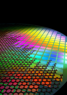 |
| This is graphene integrated onto CMOS pixels. CREDIT Fabien Vialla |
Abstract:
Silicon based CMOS (Complementary metal-oxide semiconductors) technology has truly shaped our world. It enables most of the electronics that we rely on today including computers, smartphones and digital cameras. However, to continue the path of progress in the electronics industry new technology must be developed and a key feature of this is the ability to integrate CMOS with other semiconductors. Now, Graphene Flagship researchers from ICFO (The Institute of Photonic Sciences in Barcelona) have shown that it is possible to integrate graphene into a CMOS integrated circuit.
Seeing the invisible with a graphene-CMOS integrated device
Perth, Australia | Posted on June 6th, 2017In their paper published in the journal Nature Photonics they combine this graphene-CMOS device with quantum dots to create an array of photodetectors, producing a high resolution image sensor. When used as a digital camera this device is able to sense UV, visible and infrared light at the same time. This is just one example of how this device might be used, others include in microelectronics, sensor arrays and low-power photonics.
"The development of this monolithic CMOS-based image sensor represents a milestone for low-cost, high-resolution broadband and hyperspectral imaging systems" ICREA Professor at ICFO, Frank Koppens, highlights. He assures that "in general, graphene-CMOS technology will enable a vast amount of applications, that range from safety, security, low cost pocket and smartphone cameras, fire control systems, passive night vision and night surveillance cameras, automotive sensor systems, medical imaging applications, food and pharmaceutical inspection to environmental monitoring, to name a few".
These results were enabled by the collaboration between Graphene Flagship Partner Graphenea (a Spanish graphene supplier) and ICFO, within the optoelectronics workpackage of the Graphene Flagship.
By creating a hybrid graphene and quantum dot system on a CMOS wafer using a layering and patterning approach, the Flagship team solved a complex problem with a simple solution. First the graphene is deposited, then patterned to define the pixel shape and finally a layer of PbS colloidal quantum dots is added. The photoresponse of this system is based on a photogating effect, which starts as the quantum dot layer absorbs light and transfers it as photo-generated holes or electrons to the graphene, where they circulate due to a bias voltage applied between two pixel contacts. The photo signal is then sensed by the change in conductivity of the graphene, with graphene's high charge mobility allowing for the high sensitivity of the device.
As Stijn Goossens comments, "No complex material processing or growth processes were required to achieve this graphene-quantum dot CMOS image sensor. It proved easy and cheap to fabricate at room temperature and under ambient conditions, which signifies a considerable decrease in production costs. Even more, because of its properties, it can be easily integrated on flexible substrates as well as CMOS-type integrated circuits."
The commercial applications of this research and the potential for imaging and sensing technology are now being explored in ICFO's Launchpad incubator.
Professor Andrea Ferrari, Science and Technology Officer and Chair of the Management Panel of the Graphene Flagship added: "The integration of graphene with CMOS technology is a cornerstone for the future implementation of graphene in consumer electronics. This work is a key first step, clearly demonstrating the feasibility of this approach. The Flagship has put a significant investment in the system level integration of graphene, and this will increase as we move along the technology and innovation roadmap".
####
For more information, please click here
Contacts:
Sian Fogden
44-122-376-2418
Copyright © Graphene Flagship
If you have a comment, please Contact us.Issuers of news releases, not 7th Wave, Inc. or Nanotechnology Now, are solely responsible for the accuracy of the content.
Bookmark:


| Related Links |
| Related News Press |
News and information
![]() Quantum computer improves AI predictions April 17th, 2026
Quantum computer improves AI predictions April 17th, 2026
![]() Flexible sensor gains sensitivity under pressure April 17th, 2026
Flexible sensor gains sensitivity under pressure April 17th, 2026
![]() A reusable chip for particulate matter sensing April 17th, 2026
A reusable chip for particulate matter sensing April 17th, 2026
![]() Detecting vibrational quantum beating in the predissociation dynamics of SF6 using time-resolved photoelectron spectroscopy April 17th, 2026
Detecting vibrational quantum beating in the predissociation dynamics of SF6 using time-resolved photoelectron spectroscopy April 17th, 2026
Graphene/ Graphite
![]() Electrifying results shed light on graphene foam as a potential material for lab grown cartilage June 6th, 2025
Electrifying results shed light on graphene foam as a potential material for lab grown cartilage June 6th, 2025
![]() Breakthrough in proton barrier films using pore-free graphene oxide: Kumamoto University researchers achieve new milestone in advanced coating technologies September 13th, 2024
Breakthrough in proton barrier films using pore-free graphene oxide: Kumamoto University researchers achieve new milestone in advanced coating technologies September 13th, 2024
Hardware
![]() The present and future of computing get a boost from new research July 21st, 2023
The present and future of computing get a boost from new research July 21st, 2023
![]() A Carbon Nanotube Microprocessor Mature Enough to Say Hello: Three new breakthroughs make commercial nanotube processors possible March 2nd, 2020
A Carbon Nanotube Microprocessor Mature Enough to Say Hello: Three new breakthroughs make commercial nanotube processors possible March 2nd, 2020
![]() Powering the future: Smallest all-digital circuit opens doors to 5 nm next-gen semiconductor February 11th, 2020
Powering the future: Smallest all-digital circuit opens doors to 5 nm next-gen semiconductor February 11th, 2020
Possible Futures
![]() A fundamentally new therapeutic approach to cystic fibrosis: Nanobody repairs cellular defect April 17th, 2026
A fundamentally new therapeutic approach to cystic fibrosis: Nanobody repairs cellular defect April 17th, 2026
![]() UC Irvine physicists discover method to reverse �quantum scrambling� : The work addresses the problem of information loss in quantum computing system April 17th, 2026
UC Irvine physicists discover method to reverse �quantum scrambling� : The work addresses the problem of information loss in quantum computing system April 17th, 2026
Chip Technology
![]() A reusable chip for particulate matter sensing April 17th, 2026
A reusable chip for particulate matter sensing April 17th, 2026
![]() Metasurfaces smooth light to boost magnetic sensing precision January 30th, 2026
Metasurfaces smooth light to boost magnetic sensing precision January 30th, 2026
Nanoelectronics
![]() Lab to industry: InSe wafer-scale breakthrough for future electronics August 8th, 2025
Lab to industry: InSe wafer-scale breakthrough for future electronics August 8th, 2025
![]() Interdisciplinary: Rice team tackles the future of semiconductors Multiferroics could be the key to ultralow-energy computing October 6th, 2023
Interdisciplinary: Rice team tackles the future of semiconductors Multiferroics could be the key to ultralow-energy computing October 6th, 2023
![]() Key element for a scalable quantum computer: Physicists from Forschungszentrum J�lich and RWTH Aachen University demonstrate electron transport on a quantum chip September 23rd, 2022
Key element for a scalable quantum computer: Physicists from Forschungszentrum J�lich and RWTH Aachen University demonstrate electron transport on a quantum chip September 23rd, 2022
![]() Reduced power consumption in semiconductor devices September 23rd, 2022
Reduced power consumption in semiconductor devices September 23rd, 2022
Discoveries
![]() Quantum computer improves AI predictions April 17th, 2026
Quantum computer improves AI predictions April 17th, 2026
![]() Flexible sensor gains sensitivity under pressure April 17th, 2026
Flexible sensor gains sensitivity under pressure April 17th, 2026
![]() A reusable chip for particulate matter sensing April 17th, 2026
A reusable chip for particulate matter sensing April 17th, 2026
![]() Detecting vibrational quantum beating in the predissociation dynamics of SF6 using time-resolved photoelectron spectroscopy April 17th, 2026
Detecting vibrational quantum beating in the predissociation dynamics of SF6 using time-resolved photoelectron spectroscopy April 17th, 2026
Announcements
![]() A fundamentally new therapeutic approach to cystic fibrosis: Nanobody repairs cellular defect April 17th, 2026
A fundamentally new therapeutic approach to cystic fibrosis: Nanobody repairs cellular defect April 17th, 2026
![]() UC Irvine physicists discover method to reverse �quantum scrambling� : The work addresses the problem of information loss in quantum computing system April 17th, 2026
UC Irvine physicists discover method to reverse �quantum scrambling� : The work addresses the problem of information loss in quantum computing system April 17th, 2026
Interviews/Book Reviews/Essays/Reports/Podcasts/Journals/White papers/Posters
![]() A fundamentally new therapeutic approach to cystic fibrosis: Nanobody repairs cellular defect April 17th, 2026
A fundamentally new therapeutic approach to cystic fibrosis: Nanobody repairs cellular defect April 17th, 2026
![]() UC Irvine physicists discover method to reverse �quantum scrambling� : The work addresses the problem of information loss in quantum computing system April 17th, 2026
UC Irvine physicists discover method to reverse �quantum scrambling� : The work addresses the problem of information loss in quantum computing system April 17th, 2026
|
|
||
|
|
||
| The latest news from around the world, FREE | ||
|
|
||
|
|
||
| Premium Products | ||
|
|
||
|
Only the news you want to read!
Learn More |
||
|
|
||
|
Full-service, expert consulting
Learn More |
||
|
|
||