Home > Press > Creating atomic scale nanoribbons: Researchers have demonstrated the first important step toward integrating atomically precise graphene nanoribbons (APGNRs) onto nonmetallic substrates
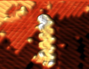 |
| Researchers have made the first important step toward integrating atomically precise graphene nanoribbons (APGNRs) onto nonmetallic substrates. CREDIT Adrian Radocea, Beckman Institute for Advanced Science and Technology |
Abstract:
Silicon crystals are the semiconductors most commonly used to make transistors, which are critical electronic components used to carry out logic operations in computing. However, as faster and more powerful processors are created, silicon has reached a performance limit: the faster it conducts electricity, the hotter it gets, leading to overheating.
Creating atomic scale nanoribbons: Researchers have demonstrated the first important step toward integrating atomically precise graphene nanoribbons (APGNRs) onto nonmetallic substrates
Urbana, IL | Posted on January 26th, 2017Graphene, made of a single-atom-thick sheet of carbon, stays much cooler and can conduct much faster, but it must be into smaller pieces, called nanoribbons, in order to act as a semiconductor. Despite much progress in the fabrication and characterization of nanoribbons, cleanly transferring them onto surfaces used for chip manufacturing has been a significant challenge.
A recent study conducted by researchers at the Beckman Institute for Advanced Science and Technology at the University of Illinois and the Department of Chemistry at the University of Nebraska-Lincoln has demonstrated the first important step toward integrating atomically precise graphene nanoribbons (APGNRs) onto nonmetallic substrates. The paper, "Solution-Synthesized Chevron Graphene Nanoribbons Exfoliated onto H:Si(100)," was published in Nano Letters.
Graphene nanoribbons measure only several nanometers across, beyond the limits of conventional chip top-down patterning used in chip manufacturing. As a result, when carved from larger pieces of graphene by various nanofabrication approaches, graphene nanoribbons are neither uniform nor narrow enough to exhibit the desired semiconductor properties.
"When you're going from the top-down, it's very hard to get control over the width. It turns out that if the width modulates by just an atom or two, the properties change significantly," said Adrian Radocea, a doctoral student in Beckman's Nanoelectronics and Nanomaterials Group.
As a result, the nanoribbons must be made from "the bottom up," from smaller molecules to create atomically precise nanoribbons with highly uniform electronic properties.
"It's like molecular building blocks: kind of like snapping Legos together to building something," said Radocea. "They lock in place, and you end up with the exact control over the ribbon width."
The "bottom-up" approach was first shown for graphene nanoribbons by Cai et al. in a 2010 Nature paper demonstrating the growth of atomically precise graphene nanoribbons on metallic substrates. In 2014, the research group of Alexander Sinitskii at the University of Nebraska-Lincoln developed an alternative approach for making atomically precise graphene nanoribbons in solution.
"The previously demonstrated synthesis on metallic substrates yields graphene nanoribbons of very high quality, but their number is rather small, as the growth it limited to the precious metal's surface," said Sinitskii, associate professor of chemistry at University of Nebraska-Lincoln and an author of the study. "It is difficult to scale this synthesis up. In contrast, when nanoribbons are synthesized in the unrestricted three-dimensional solution environment, they can be produced in large quantities."
The difficulty in cleanly transferring nanoribbons stems from the high sensitivity to environmental contaminants. Both solution-synthesized and surface-grown nanoribbons are exposed to chemicals during the transfer process that can affect the performance of graphene nanoribbon devices. To overcome this challenge, the interdisciplinary team used a dry transfer in an ultra-high vacuum environment.
A fiberglass applicator coated in graphene nanoribbon powder was heated to remove contaminants and solvent residue and then pressed onto a freshly prepared hydrogen-passivated silicon surface. The nanoribbons were studied in great detail with ultra-high vacuum scanning tunneling microscope developed by Joseph Lyding, professor of electrical and computer engineering at Illinois and an author of the study. The researchers obtained atomic-scale images and electronic measurements of the graphene nanoribbons that were critical for confirming their electronic properties and understanding the influence of the substrate.
Computational expertise available at Beckman, Radocea explained, was instrumental in understanding the experimental results. "I was still collecting more data trying to figure out what was going on. Once the modeling results came in and we started looking at the data differently, it all made sense."
Members of Beckman's Computational Multiscale Nanosystems Group, Tao Sun, a doctoral student, and Narayana Aluru, professor of mechanical science and engineering, provided expertise in computational modeling via density functional theory to investigate the properties of the nanoribbons.
"Density functional theory calculations provided a deeper understanding of the electronic properties of the integrated system and the interactions between graphene nanoribbons and the silicon substrate," said Sun. "It was exciting that the computational results could help explain and confirm the experimental results and provided a coherent story."
"Atomically precise graphene nanoribbons (APGNRs) are serious candidates for the post-silicon era when conventional silicon transistor scaling fails," said Lyding. "This demonstrates the first important step toward integrating APGNRs with technologically relevant silicon substrates."
"I find the project very exciting because you are building things with atomic level control, so you try to put every atom exactly where you want it to go," said Radocea. "There aren't many materials out there where you can say you have that ability. Nanoribbons are exciting because there is a real need and a real application."
###
The work on the synthesis of GNRs was supported by the National Science Foundation (NSF) through CHE-1455330 and by the Office of Naval Research (ONR) through N00014-16-1-2899. The materials characterization of GNRs was performed in part in Central Facilities of the Nebraska Center for Materials and Nanoscience (NCMN), which is supported by the Nebraska Research Initiative. The STM work by A.R. and J.W.L. was supported by the Office of Naval Research under grant # N00014-13-1-0300. T.S. and N.R.A. are supported by AFOSR under grant # FA9550-12-1-0464 and by NSF under grants 1264282, 1420882, 1506619, and 1545907.
####
For more information, please click here
Contacts:
Maeve Reilly
217-244-7316
Copyright © Beckman Institute for Advanced Science and Technology
If you have a comment, please Contact us.Issuers of news releases, not 7th Wave, Inc. or Nanotechnology Now, are solely responsible for the accuracy of the content.
Bookmark:


| Related Links |
| Related News Press |
News and information
![]() Quantum computer improves AI predictions April 17th, 2026
Quantum computer improves AI predictions April 17th, 2026
![]() Flexible sensor gains sensitivity under pressure April 17th, 2026
Flexible sensor gains sensitivity under pressure April 17th, 2026
![]() A reusable chip for particulate matter sensing April 17th, 2026
A reusable chip for particulate matter sensing April 17th, 2026
![]() Detecting vibrational quantum beating in the predissociation dynamics of SF6 using time-resolved photoelectron spectroscopy April 17th, 2026
Detecting vibrational quantum beating in the predissociation dynamics of SF6 using time-resolved photoelectron spectroscopy April 17th, 2026
2 Dimensional Materials
![]() Flexible sensor gains sensitivity under pressure April 17th, 2026
Flexible sensor gains sensitivity under pressure April 17th, 2026
Graphene/ Graphite
![]() Electrifying results shed light on graphene foam as a potential material for lab grown cartilage June 6th, 2025
Electrifying results shed light on graphene foam as a potential material for lab grown cartilage June 6th, 2025
![]() Breakthrough in proton barrier films using pore-free graphene oxide: Kumamoto University researchers achieve new milestone in advanced coating technologies September 13th, 2024
Breakthrough in proton barrier films using pore-free graphene oxide: Kumamoto University researchers achieve new milestone in advanced coating technologies September 13th, 2024
Hardware
![]() The present and future of computing get a boost from new research July 21st, 2023
The present and future of computing get a boost from new research July 21st, 2023
![]() A Carbon Nanotube Microprocessor Mature Enough to Say Hello: Three new breakthroughs make commercial nanotube processors possible March 2nd, 2020
A Carbon Nanotube Microprocessor Mature Enough to Say Hello: Three new breakthroughs make commercial nanotube processors possible March 2nd, 2020
![]() Powering the future: Smallest all-digital circuit opens doors to 5 nm next-gen semiconductor February 11th, 2020
Powering the future: Smallest all-digital circuit opens doors to 5 nm next-gen semiconductor February 11th, 2020
Govt.-Legislation/Regulation/Funding/Policy
![]() Quantum computer improves AI predictions April 17th, 2026
Quantum computer improves AI predictions April 17th, 2026
![]() Metasurfaces smooth light to boost magnetic sensing precision January 30th, 2026
Metasurfaces smooth light to boost magnetic sensing precision January 30th, 2026
![]() New imaging approach transforms study of bacterial biofilms August 8th, 2025
New imaging approach transforms study of bacterial biofilms August 8th, 2025
Possible Futures
![]() A fundamentally new therapeutic approach to cystic fibrosis: Nanobody repairs cellular defect April 17th, 2026
A fundamentally new therapeutic approach to cystic fibrosis: Nanobody repairs cellular defect April 17th, 2026
![]() UC Irvine physicists discover method to reverse �quantum scrambling� : The work addresses the problem of information loss in quantum computing system April 17th, 2026
UC Irvine physicists discover method to reverse �quantum scrambling� : The work addresses the problem of information loss in quantum computing system April 17th, 2026
Chip Technology
![]() A reusable chip for particulate matter sensing April 17th, 2026
A reusable chip for particulate matter sensing April 17th, 2026
![]() Metasurfaces smooth light to boost magnetic sensing precision January 30th, 2026
Metasurfaces smooth light to boost magnetic sensing precision January 30th, 2026
Nanoelectronics
![]() Lab to industry: InSe wafer-scale breakthrough for future electronics August 8th, 2025
Lab to industry: InSe wafer-scale breakthrough for future electronics August 8th, 2025
![]() Interdisciplinary: Rice team tackles the future of semiconductors Multiferroics could be the key to ultralow-energy computing October 6th, 2023
Interdisciplinary: Rice team tackles the future of semiconductors Multiferroics could be the key to ultralow-energy computing October 6th, 2023
![]() Key element for a scalable quantum computer: Physicists from Forschungszentrum J�lich and RWTH Aachen University demonstrate electron transport on a quantum chip September 23rd, 2022
Key element for a scalable quantum computer: Physicists from Forschungszentrum J�lich and RWTH Aachen University demonstrate electron transport on a quantum chip September 23rd, 2022
![]() Reduced power consumption in semiconductor devices September 23rd, 2022
Reduced power consumption in semiconductor devices September 23rd, 2022
Discoveries
![]() Quantum computer improves AI predictions April 17th, 2026
Quantum computer improves AI predictions April 17th, 2026
![]() Flexible sensor gains sensitivity under pressure April 17th, 2026
Flexible sensor gains sensitivity under pressure April 17th, 2026
![]() A reusable chip for particulate matter sensing April 17th, 2026
A reusable chip for particulate matter sensing April 17th, 2026
![]() Detecting vibrational quantum beating in the predissociation dynamics of SF6 using time-resolved photoelectron spectroscopy April 17th, 2026
Detecting vibrational quantum beating in the predissociation dynamics of SF6 using time-resolved photoelectron spectroscopy April 17th, 2026
Announcements
![]() A fundamentally new therapeutic approach to cystic fibrosis: Nanobody repairs cellular defect April 17th, 2026
A fundamentally new therapeutic approach to cystic fibrosis: Nanobody repairs cellular defect April 17th, 2026
![]() UC Irvine physicists discover method to reverse �quantum scrambling� : The work addresses the problem of information loss in quantum computing system April 17th, 2026
UC Irvine physicists discover method to reverse �quantum scrambling� : The work addresses the problem of information loss in quantum computing system April 17th, 2026
Interviews/Book Reviews/Essays/Reports/Podcasts/Journals/White papers/Posters
![]() A fundamentally new therapeutic approach to cystic fibrosis: Nanobody repairs cellular defect April 17th, 2026
A fundamentally new therapeutic approach to cystic fibrosis: Nanobody repairs cellular defect April 17th, 2026
![]() UC Irvine physicists discover method to reverse �quantum scrambling� : The work addresses the problem of information loss in quantum computing system April 17th, 2026
UC Irvine physicists discover method to reverse �quantum scrambling� : The work addresses the problem of information loss in quantum computing system April 17th, 2026
Military
![]() Quantum engineers �squeeze� laser frequency combs to make more sensitive gas sensors January 17th, 2025
Quantum engineers �squeeze� laser frequency combs to make more sensitive gas sensors January 17th, 2025
![]() Chainmail-like material could be the future of armor: First 2D mechanically interlocked polymer exhibits exceptional flexibility and strength January 17th, 2025
Chainmail-like material could be the future of armor: First 2D mechanically interlocked polymer exhibits exceptional flexibility and strength January 17th, 2025
![]() Single atoms show their true color July 5th, 2024
Single atoms show their true color July 5th, 2024
![]() NRL charters Navy�s quantum inertial navigation path to reduce drift April 5th, 2024
NRL charters Navy�s quantum inertial navigation path to reduce drift April 5th, 2024
Grants/Sponsored Research/Awards/Scholarships/Gifts/Contests/Honors/Records
![]() Quantum computer improves AI predictions April 17th, 2026
Quantum computer improves AI predictions April 17th, 2026
![]() Detecting vibrational quantum beating in the predissociation dynamics of SF6 using time-resolved photoelectron spectroscopy April 17th, 2026
Detecting vibrational quantum beating in the predissociation dynamics of SF6 using time-resolved photoelectron spectroscopy April 17th, 2026
![]() Metasurfaces smooth light to boost magnetic sensing precision January 30th, 2026
Metasurfaces smooth light to boost magnetic sensing precision January 30th, 2026
Research partnerships
![]() Lab to industry: InSe wafer-scale breakthrough for future electronics August 8th, 2025
Lab to industry: InSe wafer-scale breakthrough for future electronics August 8th, 2025
![]() HKU physicists uncover hidden order in the quantum world through deconfined quantum critical points April 25th, 2025
HKU physicists uncover hidden order in the quantum world through deconfined quantum critical points April 25th, 2025
|
|
||
|
|
||
| The latest news from around the world, FREE | ||
|
|
||
|
|
||
| Premium Products | ||
|
|
||
|
Only the news you want to read!
Learn More |
||
|
|
||
|
Full-service, expert consulting
Learn More |
||
|
|
||