Home > Press > Illinois team advances GaN-on-Silicon for scalable high electron mobility transistors
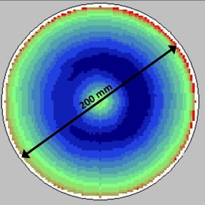 |
| This is a GaN on 200 mm Si wafer thickness mapping image. CREDIT University of Illinois |
Abstract:
A team of researchers at the University of Illinois at Urbana-Champaign has advanced gallium nitride (GaN)-on-silicon transistor technology by optimizing the composition of the semiconductor layers that make up the device. Working with industry partners Veeco and IBM, the team created the high electron mobility transistor (HEMT) structure on a 200 mm silicon substrate with a process that will scale to larger industry-standard wafer sizes.
Illinois team advances GaN-on-Silicon for scalable high electron mobility transistors
Urbana, IL | Posted on January 10th, 2017Can Bayram, an assistant professor of electrical and computer engineering (ECE), and his team have created the GaN HEMT structure on a silicon platform because it is compatible with existing CMOS manufacturing processes and is less expensive than other substrate options like sapphire and silicon carbide.
However, silicon does have its challenges. Namely, the lattice constant, or space between silicon atoms, doesn't match up with the atomic structure of the GaN grown on top of it.
"When you grow the GaN on top, there's a lot of strain between the layers, so we grew buffer layers [between the silicon and GaN] to help change the lattice constant into the proper size," explained ECE undergraduate researcher Josh Perozek, lead author of the group's paper, "Investigation of structural, optical, and electrical characteristics of an AlGaN/GaN high electron mobility transistor structure across a 200mm Si(1 1 1) substrate," in the Journal of Physics D: Applied Physics.
Without these buffer layers, cracks or other defects will form in the GaN material, which would prevent the transistor from operating properly. Specifically, these defects -- threading dislocations or holes where atoms should be--ruin the properties of the 2-dimensional electron gas channel in the device. This channel is critical to the HEMTs ability to conduct current and function at high frequencies.
"The single most important thing for these GaN [HEMT] devices is to have high 2D electron gas concentration," said Bayram, about the accumulation of electrons in a channel at the interface between the silicon and the various GaN-based layers above it.
"The problem is you have to control the strain balance among all those layers--from substrate all the way up to the channel -- so as to maximize the density of the of the conducting electrons in order to get the fastest transistor with the highest possible power density."
After studying three different buffer layer configurations, Bayram's team discovered that thicker buffer layers made of graded AlGaN reduce threading dislocation, and stacking those layers reduces stress. With this type of configuration, the team achieved an electron mobility of 1,800 cm2/V-sec.
"The less strain there is on the GaN layer, the higher the mobility will be, which ultimately corresponds to higher transistor operating frequencies," said Hsuan-Ping Lee, an ECE graduate student researcher leading the scaling of these devices for 5G applications.
According to Bayram, the next step for his team is to fabricate fully functional high-frequency GaN HEMTs on a silicon platform for use in the 5G wireless data networks.
When it's fully deployed, the 5G network will enable faster data rates for the world's 8 billion mobile phones, and will provide better connectivity and performance for Internet of Things (IoT) devices and driverless cars.
###
The team, in collaboration with Veeco and IBM, conducted their research at the University of Illinois Micro + Nanotechnology Lab with support from the Air Force Office of Scientific Research.
####
For more information, please click here
Contacts:
Can Bayram
217-300-0978
Copyright © University of Illinois College of Engineering
If you have a comment, please Contact us.Issuers of news releases, not 7th Wave, Inc. or Nanotechnology Now, are solely responsible for the accuracy of the content.
Bookmark:


| Related Links |
| Related News Press |
News and information
![]() Quantum computer improves AI predictions April 17th, 2026
Quantum computer improves AI predictions April 17th, 2026
![]() Flexible sensor gains sensitivity under pressure April 17th, 2026
Flexible sensor gains sensitivity under pressure April 17th, 2026
![]() A reusable chip for particulate matter sensing April 17th, 2026
A reusable chip for particulate matter sensing April 17th, 2026
![]() Detecting vibrational quantum beating in the predissociation dynamics of SF6 using time-resolved photoelectron spectroscopy April 17th, 2026
Detecting vibrational quantum beating in the predissociation dynamics of SF6 using time-resolved photoelectron spectroscopy April 17th, 2026
Wireless/telecommunications/RF/Antennas/Microwaves
![]() Researchers develop molecular qubits that communicate at telecom frequencies October 3rd, 2025
Researchers develop molecular qubits that communicate at telecom frequencies October 3rd, 2025
![]() HKUST researchers develop new integration technique for efficient coupling of III-V and silicon February 16th, 2024
HKUST researchers develop new integration technique for efficient coupling of III-V and silicon February 16th, 2024
Internet-of-Things
![]() Nanofibrous metal oxide semiconductor for sensory face November 8th, 2024
Nanofibrous metal oxide semiconductor for sensory face November 8th, 2024
Govt.-Legislation/Regulation/Funding/Policy
![]() Quantum computer improves AI predictions April 17th, 2026
Quantum computer improves AI predictions April 17th, 2026
![]() Metasurfaces smooth light to boost magnetic sensing precision January 30th, 2026
Metasurfaces smooth light to boost magnetic sensing precision January 30th, 2026
![]() New imaging approach transforms study of bacterial biofilms August 8th, 2025
New imaging approach transforms study of bacterial biofilms August 8th, 2025
Possible Futures
![]() A fundamentally new therapeutic approach to cystic fibrosis: Nanobody repairs cellular defect April 17th, 2026
A fundamentally new therapeutic approach to cystic fibrosis: Nanobody repairs cellular defect April 17th, 2026
![]() UC Irvine physicists discover method to reverse �quantum scrambling� : The work addresses the problem of information loss in quantum computing system April 17th, 2026
UC Irvine physicists discover method to reverse �quantum scrambling� : The work addresses the problem of information loss in quantum computing system April 17th, 2026
Chip Technology
![]() A reusable chip for particulate matter sensing April 17th, 2026
A reusable chip for particulate matter sensing April 17th, 2026
![]() Metasurfaces smooth light to boost magnetic sensing precision January 30th, 2026
Metasurfaces smooth light to boost magnetic sensing precision January 30th, 2026
Discoveries
![]() Quantum computer improves AI predictions April 17th, 2026
Quantum computer improves AI predictions April 17th, 2026
![]() Flexible sensor gains sensitivity under pressure April 17th, 2026
Flexible sensor gains sensitivity under pressure April 17th, 2026
![]() A reusable chip for particulate matter sensing April 17th, 2026
A reusable chip for particulate matter sensing April 17th, 2026
![]() Detecting vibrational quantum beating in the predissociation dynamics of SF6 using time-resolved photoelectron spectroscopy April 17th, 2026
Detecting vibrational quantum beating in the predissociation dynamics of SF6 using time-resolved photoelectron spectroscopy April 17th, 2026
Announcements
![]() A fundamentally new therapeutic approach to cystic fibrosis: Nanobody repairs cellular defect April 17th, 2026
A fundamentally new therapeutic approach to cystic fibrosis: Nanobody repairs cellular defect April 17th, 2026
![]() UC Irvine physicists discover method to reverse �quantum scrambling� : The work addresses the problem of information loss in quantum computing system April 17th, 2026
UC Irvine physicists discover method to reverse �quantum scrambling� : The work addresses the problem of information loss in quantum computing system April 17th, 2026
Interviews/Book Reviews/Essays/Reports/Podcasts/Journals/White papers/Posters
![]() A fundamentally new therapeutic approach to cystic fibrosis: Nanobody repairs cellular defect April 17th, 2026
A fundamentally new therapeutic approach to cystic fibrosis: Nanobody repairs cellular defect April 17th, 2026
![]() UC Irvine physicists discover method to reverse �quantum scrambling� : The work addresses the problem of information loss in quantum computing system April 17th, 2026
UC Irvine physicists discover method to reverse �quantum scrambling� : The work addresses the problem of information loss in quantum computing system April 17th, 2026
Military
![]() Quantum engineers �squeeze� laser frequency combs to make more sensitive gas sensors January 17th, 2025
Quantum engineers �squeeze� laser frequency combs to make more sensitive gas sensors January 17th, 2025
![]() Chainmail-like material could be the future of armor: First 2D mechanically interlocked polymer exhibits exceptional flexibility and strength January 17th, 2025
Chainmail-like material could be the future of armor: First 2D mechanically interlocked polymer exhibits exceptional flexibility and strength January 17th, 2025
![]() Single atoms show their true color July 5th, 2024
Single atoms show their true color July 5th, 2024
![]() NRL charters Navy�s quantum inertial navigation path to reduce drift April 5th, 2024
NRL charters Navy�s quantum inertial navigation path to reduce drift April 5th, 2024
Automotive/Transportation
![]() Decoding hydrogen‑bond network of electrolyte for cryogenic durable aqueous zinc‑ion batteries January 30th, 2026
Decoding hydrogen‑bond network of electrolyte for cryogenic durable aqueous zinc‑ion batteries January 30th, 2026
![]() Sensors innovations for smart lithium-based batteries: advancements, opportunities, and potential challenges August 8th, 2025
Sensors innovations for smart lithium-based batteries: advancements, opportunities, and potential challenges August 8th, 2025
![]() Simple algorithm paired with standard imaging tool could predict failure in lithium metal batteries August 8th, 2025
Simple algorithm paired with standard imaging tool could predict failure in lithium metal batteries August 8th, 2025
|
|
||
|
|
||
| The latest news from around the world, FREE | ||
|
|
||
|
|
||
| Premium Products | ||
|
|
||
|
Only the news you want to read!
Learn More |
||
|
|
||
|
Full-service, expert consulting
Learn More |
||
|
|
||