Home > Press > Electron beam microscope directly writes nanoscale features in liquid with metal ink
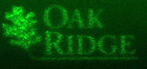 |
| To direct-write the logo of the Department of Energy�s Oak Ridge National Laboratory, scientists started with a gray-scale image. They used the electron beam of an aberration-corrected scanning transmission electron microscope to induce palladium from a solution to deposit as nanocrystals. Image credit: Oak Ridge National Laboratory, U.S. Dept. of Energy |
Abstract:
Scientists at the Department of Energy's Oak Ridge National Laboratory are the first to harness a scanning transmission electron microscope (STEM) to directly write tiny patterns in metallic "ink," forming features in liquid that are finer than half the width of a human hair.
Electron beam microscope directly writes nanoscale features in liquid with metal ink
Oak Ridge, TN | Posted on September 16th, 2016The automated process is controlled by weaving a STEM instrument's electron beam through a liquid-filled cell to spur deposition of metal onto a silicon microchip. The patterns created are "nanoscale," or on the size scale of atoms or molecules.
Usually fabrication of nanoscale patterns requires lithography, which employs masks to prevent material from accumulating on protected areas. ORNL's new direct-write technology is like lithography without the mask.
Details of this unique capability are published online in Nanoscale, a journal of the Royal Society of Chemistry, and researchers are applying for a patent. The technique may provide a new way to tailor devices for electronics and other applications.
"We can now deposit high-purity metals at specific sites to build structures, with tailored material properties for a specific application," said lead author Raymond Unocic of the Center for Nanophase Materials Sciences (CNMS), a DOE Office of Science User Facility at ORNL. "We can customize architectures and chemistries. We're only limited by systems that are dissolvable in the liquid and can undergo chemical reactions."
The experimenters used grayscale images to create nanoscale templates. Then they beamed electrons into a cell filled with a solution containing palladium chloride. Pure palladium separated out and deposited wherever the electron beam passed.
Liquid environments are a must for chemistry. Researchers first needed a way to encapsulate the liquid so the extreme dryness of the vacuum inside the microscope would not evaporate the liquid. The researchers started with a cell made of microchips with a silicon nitride membrane to serve as a window through which the electron beam could pass.
Then they needed to elicit a new capability from a STEM instrument. "It's one thing to utilize a microscope for imaging and spectroscopy. It's another to take control of that microscope to perform controlled and site-specific nanoscale chemical reactions," Unocic said. "With other techniques for electron-beam lithography, there are ways to interface that microscope where you can control the beam. But this isn't the way that aberration-corrected scanning transmission electron microscopes are set up."
Enter Stephen Jesse, leader of CNMS's Directed Nanoscale Transformations theme. This group looks at tools that scientists use to see and understand matter and its nanoscale properties in a new light, and explores whether those tools can also transform matter one atom at a time and build structures with specified functions. "Think of what we are doing as working in nanoscale laboratories," Jesse said. "This means being able to induce and stop reactions at will, as well as monitor them while they are happening."
Jesse had recently developed a system that serves as an interface between a nanolithography pattern and a STEM's scan coils, and ORNL researchers had already used it to selectively transform solids. The microscope focuses the electron beam to a fine point, which microscopists could move just by taking control of the scan coils. Unocic with Andrew Lupini, Albina Borisevich and Sergei Kalinin integrated Jesse's scan control/nanolithography system within the microscope so that they could control the beam entering the liquid cell. David Cullen performed subsequent chemical analysis.
"This beam-induced nanolithography relies critically on controlling chemical reactions in nanoscale volumes with a beam of energetic electrons," said Jesse. The system controls electron-beam position, speed and dose. The dose--how many electrons are being pumped into the system--governs how fast chemicals are transformed.
This nanoscale technology is similar to larger-scale activities, such as using electron beams to transform materials for 3D printing at ORNL's Manufacturing Demonstration Facility. In that case, an electron beam melts powder so that it solidifies, layer by layer, to create an object.
"We're essentially doing the same thing, but within a liquid," Unocic said. "Now we can create structures from a liquid-phase precursor solution in the shape that we want and the chemistry that we want, tuning the physiochemical properties for a given application."
Precise control of the beam position and the electron dose produces tailored architectures. Encapsulating different liquids and sequentially flowing them during patterning customizes the chemistry too.
The current resolution of metallic "pixels" the liquid ink can direct-write is 40 nanometers, or twice the width of an influenza virus. In future work, Unocic and colleagues would like to push the resolution down to approach the state of the art of conventional nanolithography, 10 nanometers. They would also like to fabricate multi-component structures.
The title of the paper is "Direct-write liquid phase transformations with a scanning transmission electron microscope."
###
This research was conducted at the Center for Nanophase Materials Sciences, a DOE Office of Science User Facility at ORNL. The DOE Office of Science supported the work. ORNL Laboratory Directed Research and Development funds supported a portion of the work.
####
About Oak Ridge National Laboratory
UT-Battelle manages ORNL for DOE's Office of Science. The single largest supporter of basic research in the physical sciences in the United States, the Office of Science is working to address some of the most pressing challenges of our time. For more information, please visit www.science.energy.gov
For more information, please click here
Contacts:
Dawn Levy
865-576-6448
Copyright © Oak Ridge National Laboratory
If you have a comment, please Contact us.Issuers of news releases, not 7th Wave, Inc. or Nanotechnology Now, are solely responsible for the accuracy of the content.
Bookmark:


| Related Links |
| Related News Press |
News and information
![]() Quantum computer improves AI predictions April 17th, 2026
Quantum computer improves AI predictions April 17th, 2026
![]() Flexible sensor gains sensitivity under pressure April 17th, 2026
Flexible sensor gains sensitivity under pressure April 17th, 2026
![]() A reusable chip for particulate matter sensing April 17th, 2026
A reusable chip for particulate matter sensing April 17th, 2026
![]() Detecting vibrational quantum beating in the predissociation dynamics of SF6 using time-resolved photoelectron spectroscopy April 17th, 2026
Detecting vibrational quantum beating in the predissociation dynamics of SF6 using time-resolved photoelectron spectroscopy April 17th, 2026
Imaging
![]() Simple algorithm paired with standard imaging tool could predict failure in lithium metal batteries August 8th, 2025
Simple algorithm paired with standard imaging tool could predict failure in lithium metal batteries August 8th, 2025
![]() First real-time observation of two-dimensional melting process: Researchers at Mainz University unveil new insights into magnetic vortex structures August 8th, 2025
First real-time observation of two-dimensional melting process: Researchers at Mainz University unveil new insights into magnetic vortex structures August 8th, 2025
![]() New imaging approach transforms study of bacterial biofilms August 8th, 2025
New imaging approach transforms study of bacterial biofilms August 8th, 2025
Laboratories
![]() Researchers develop molecular qubits that communicate at telecom frequencies October 3rd, 2025
Researchers develop molecular qubits that communicate at telecom frequencies October 3rd, 2025
Govt.-Legislation/Regulation/Funding/Policy
![]() Quantum computer improves AI predictions April 17th, 2026
Quantum computer improves AI predictions April 17th, 2026
![]() Metasurfaces smooth light to boost magnetic sensing precision January 30th, 2026
Metasurfaces smooth light to boost magnetic sensing precision January 30th, 2026
![]() New imaging approach transforms study of bacterial biofilms August 8th, 2025
New imaging approach transforms study of bacterial biofilms August 8th, 2025
Possible Futures
![]() A fundamentally new therapeutic approach to cystic fibrosis: Nanobody repairs cellular defect April 17th, 2026
A fundamentally new therapeutic approach to cystic fibrosis: Nanobody repairs cellular defect April 17th, 2026
![]() UC Irvine physicists discover method to reverse �quantum scrambling� : The work addresses the problem of information loss in quantum computing system April 17th, 2026
UC Irvine physicists discover method to reverse �quantum scrambling� : The work addresses the problem of information loss in quantum computing system April 17th, 2026
Chip Technology
![]() A reusable chip for particulate matter sensing April 17th, 2026
A reusable chip for particulate matter sensing April 17th, 2026
![]() Metasurfaces smooth light to boost magnetic sensing precision January 30th, 2026
Metasurfaces smooth light to boost magnetic sensing precision January 30th, 2026
Discoveries
![]() Quantum computer improves AI predictions April 17th, 2026
Quantum computer improves AI predictions April 17th, 2026
![]() Flexible sensor gains sensitivity under pressure April 17th, 2026
Flexible sensor gains sensitivity under pressure April 17th, 2026
![]() A reusable chip for particulate matter sensing April 17th, 2026
A reusable chip for particulate matter sensing April 17th, 2026
![]() Detecting vibrational quantum beating in the predissociation dynamics of SF6 using time-resolved photoelectron spectroscopy April 17th, 2026
Detecting vibrational quantum beating in the predissociation dynamics of SF6 using time-resolved photoelectron spectroscopy April 17th, 2026
Announcements
![]() A fundamentally new therapeutic approach to cystic fibrosis: Nanobody repairs cellular defect April 17th, 2026
A fundamentally new therapeutic approach to cystic fibrosis: Nanobody repairs cellular defect April 17th, 2026
![]() UC Irvine physicists discover method to reverse �quantum scrambling� : The work addresses the problem of information loss in quantum computing system April 17th, 2026
UC Irvine physicists discover method to reverse �quantum scrambling� : The work addresses the problem of information loss in quantum computing system April 17th, 2026
Interviews/Book Reviews/Essays/Reports/Podcasts/Journals/White papers/Posters
![]() A fundamentally new therapeutic approach to cystic fibrosis: Nanobody repairs cellular defect April 17th, 2026
A fundamentally new therapeutic approach to cystic fibrosis: Nanobody repairs cellular defect April 17th, 2026
![]() UC Irvine physicists discover method to reverse �quantum scrambling� : The work addresses the problem of information loss in quantum computing system April 17th, 2026
UC Irvine physicists discover method to reverse �quantum scrambling� : The work addresses the problem of information loss in quantum computing system April 17th, 2026
Tools
![]() Metasurfaces smooth light to boost magnetic sensing precision January 30th, 2026
Metasurfaces smooth light to boost magnetic sensing precision January 30th, 2026
![]() From sensors to smart systems: the rise of AI-driven photonic noses January 30th, 2026
From sensors to smart systems: the rise of AI-driven photonic noses January 30th, 2026
![]() Japan launches fully domestically produced quantum computer: Expo visitors to experience quantum computing firsthand August 8th, 2025
Japan launches fully domestically produced quantum computer: Expo visitors to experience quantum computing firsthand August 8th, 2025
|
|
||
|
|
||
| The latest news from around the world, FREE | ||
|
|
||
|
|
||
| Premium Products | ||
|
|
||
|
Only the news you want to read!
Learn More |
||
|
|
||
|
Full-service, expert consulting
Learn More |
||
|
|
||