Home > Press > Berkeley Lab scientists grow atomically thin transistors and circuits
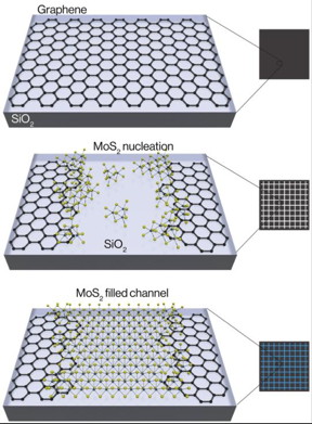 |
| This schematic shows the chemical assembly of two-dimensional crystals. Graphene is first etched into channels and the TMDC molybdenum disulfide (MoS2) begins to nucleate around the edges and within the channel. On the edges, MoS2 slightly overlaps on top of the graphene. Finally, further growth results in MoS2 completely filling the channels. CREDIT: Berkeley Lab |
Abstract:
In an advance that helps pave the way for next-generation electronics and computing technologies--and possibly paper-thin gadgets --scientists with the U.S. Department of Energy's Lawrence Berkeley National Laboratory (Berkeley Lab) developed a way to chemically assemble transistors and circuits that are only a few atoms thick.
Berkeley Lab scientists grow atomically thin transistors and circuits
Berkeley, CA | Posted on July 13th, 2016What's more, their method yields functional structures at a scale large enough to begin thinking about real-world applications and commercial scalability.
They report their research online July 11 in the journal Nature Nanotechnology.
The scientists controlled the synthesis of a transistor in which narrow channels were etched onto conducting graphene, and a semiconducting material called a transition-metal dichalcogenide, or TMDC, was seeded in the blank channels. Both of these materials are single-layered crystals and atomically thin, so the two-part assembly yielded electronic structures that are essentially two-dimensional. In addition, the synthesis is able to cover an area a few centimeters long and a few millimeters wide.
"This is a big step toward a scalable and repeatable way to build atomically thin electronics or pack more computing power in a smaller area," says Xiang Zhang, a senior scientist in Berkeley Lab's Materials Sciences Division who led the study.
Zhang also holds the Ernest S. Kuh Endowed Chair at the University of California (UC) Berkeley and is a member of the Kavli Energy NanoSciences Institute at Berkeley. Other scientists who contributed to the research include Mervin Zhao, Yu Ye, Yang Xia, Hanyu Zhu, Siqi Wang, and Yuan Wang from UC Berkeley as well as Yimo Han and David Muller from Cornell University.
Their work is part of a new wave of research aimed at keeping pace with Moore's Law, which holds that the number of transistors in an integrated circuit doubles approximately every two years. In order to keep this pace, scientists predict that integrated electronics will soon require transistors that measure less than ten nanometers in length.
Transistors are electronic switches, so they need to be able to turn on and off, which is a characteristic of semiconductors. However, at the nanometer scale, silicon transistors likely won't be a good option. That's because silicon is a bulk material, and as electronics made from silicon become smaller and smaller, their performance as switches dramatically decreases, which is a major roadblock for future electronics.
Researchers have looked to two-dimensional crystals that are only one molecule thick as alternative materials to keep up with Moore's Law. These crystals aren't subject to the constraints of silicon.
In this vein, the Berkeley Lab scientists developed a way to seed a single-layered semiconductor, in this case the TMDC molybdenum disulfide (MoS2), into channels lithographically etched within a sheet of conducting graphene. The two atomic sheets meet to form nanometer-scale junctions that enable graphene to efficiently inject current into the MoS2. These junctions make atomically thin transistors.
"This approach allows for the chemical assembly of electronic circuits, using two-dimensional materials, which show improved performance compared to using traditional metals to inject current into TMDCs," says Mervin Zhao, a lead author and Ph.D. student in Zhang's group at Berkeley Lab and UC Berkeley.
Optical and electron microscopy images, and spectroscopic mapping, confirmed various aspects related to the successful formation and functionality of the two-dimensional transistors.
In addition, the scientists demonstrated the applicability of the structure by assembling it into the logic circuitry of an inverter. This further underscores the technology's ability to lay the foundation for a chemically assembled atomic computer, the scientists say.
"Both of these two-dimensional crystals have been synthesized in the wafer scale in a way that is compatible with current semiconductor manufacturing. By integrating our technique with other growth systems, it's possible that future computing can be done completely with atomically thin crystals," says Zhao.
###
The research was supported by the Office of Naval Research and the National Science Foundation.
####
About Berkeley Lab
Lawrence Berkeley National Laboratory addresses the world's most urgent scientific challenges by advancing sustainable energy, protecting human health, creating new materials, and revealing the origin and fate of the universe. Founded in 1931, Berkeley Lab's scientific expertise has been recognized with 13 Nobel prizes. The University of California manages Berkeley Lab for the U.S. Department of Energy's Office of Science. For more, visit www.lbl.gov.
DOE's Office of Science is the single largest supporter of basic research in the physical sciences in the United States, and is working to address some of the most pressing challenges of our time. For more information, please visit science.energy.gov.
For more information, please click here
Contacts:
Jon Weiner
510-486-4014
Copyright © Berkeley Lab
If you have a comment, please Contact us.Issuers of news releases, not 7th Wave, Inc. or Nanotechnology Now, are solely responsible for the accuracy of the content.
Bookmark:


| Related News Press |
News and information
![]() Quantum computer improves AI predictions April 17th, 2026
Quantum computer improves AI predictions April 17th, 2026
![]() Flexible sensor gains sensitivity under pressure April 17th, 2026
Flexible sensor gains sensitivity under pressure April 17th, 2026
![]() A reusable chip for particulate matter sensing April 17th, 2026
A reusable chip for particulate matter sensing April 17th, 2026
![]() Detecting vibrational quantum beating in the predissociation dynamics of SF6 using time-resolved photoelectron spectroscopy April 17th, 2026
Detecting vibrational quantum beating in the predissociation dynamics of SF6 using time-resolved photoelectron spectroscopy April 17th, 2026
2 Dimensional Materials
![]() Flexible sensor gains sensitivity under pressure April 17th, 2026
Flexible sensor gains sensitivity under pressure April 17th, 2026
![]() ICFO researchers overcome long-standing bottleneck in single photon detection with twisted 2D materials August 8th, 2025
ICFO researchers overcome long-standing bottleneck in single photon detection with twisted 2D materials August 8th, 2025
![]() First real-time observation of two-dimensional melting process: Researchers at Mainz University unveil new insights into magnetic vortex structures August 8th, 2025
First real-time observation of two-dimensional melting process: Researchers at Mainz University unveil new insights into magnetic vortex structures August 8th, 2025
![]() Lab to industry: InSe wafer-scale breakthrough for future electronics August 8th, 2025
Lab to industry: InSe wafer-scale breakthrough for future electronics August 8th, 2025
Laboratories
![]() Researchers develop molecular qubits that communicate at telecom frequencies October 3rd, 2025
Researchers develop molecular qubits that communicate at telecom frequencies October 3rd, 2025
Graphene/ Graphite
![]() Electrifying results shed light on graphene foam as a potential material for lab grown cartilage June 6th, 2025
Electrifying results shed light on graphene foam as a potential material for lab grown cartilage June 6th, 2025
![]() Breakthrough in proton barrier films using pore-free graphene oxide: Kumamoto University researchers achieve new milestone in advanced coating technologies September 13th, 2024
Breakthrough in proton barrier films using pore-free graphene oxide: Kumamoto University researchers achieve new milestone in advanced coating technologies September 13th, 2024
Govt.-Legislation/Regulation/Funding/Policy
![]() Quantum computer improves AI predictions April 17th, 2026
Quantum computer improves AI predictions April 17th, 2026
![]() Metasurfaces smooth light to boost magnetic sensing precision January 30th, 2026
Metasurfaces smooth light to boost magnetic sensing precision January 30th, 2026
![]() New imaging approach transforms study of bacterial biofilms August 8th, 2025
New imaging approach transforms study of bacterial biofilms August 8th, 2025
Possible Futures
![]() A fundamentally new therapeutic approach to cystic fibrosis: Nanobody repairs cellular defect April 17th, 2026
A fundamentally new therapeutic approach to cystic fibrosis: Nanobody repairs cellular defect April 17th, 2026
![]() UC Irvine physicists discover method to reverse �quantum scrambling� : The work addresses the problem of information loss in quantum computing system April 17th, 2026
UC Irvine physicists discover method to reverse �quantum scrambling� : The work addresses the problem of information loss in quantum computing system April 17th, 2026
Chip Technology
![]() A reusable chip for particulate matter sensing April 17th, 2026
A reusable chip for particulate matter sensing April 17th, 2026
![]() Metasurfaces smooth light to boost magnetic sensing precision January 30th, 2026
Metasurfaces smooth light to boost magnetic sensing precision January 30th, 2026
Nanoelectronics
![]() Lab to industry: InSe wafer-scale breakthrough for future electronics August 8th, 2025
Lab to industry: InSe wafer-scale breakthrough for future electronics August 8th, 2025
![]() Interdisciplinary: Rice team tackles the future of semiconductors Multiferroics could be the key to ultralow-energy computing October 6th, 2023
Interdisciplinary: Rice team tackles the future of semiconductors Multiferroics could be the key to ultralow-energy computing October 6th, 2023
![]() Key element for a scalable quantum computer: Physicists from Forschungszentrum J�lich and RWTH Aachen University demonstrate electron transport on a quantum chip September 23rd, 2022
Key element for a scalable quantum computer: Physicists from Forschungszentrum J�lich and RWTH Aachen University demonstrate electron transport on a quantum chip September 23rd, 2022
![]() Reduced power consumption in semiconductor devices September 23rd, 2022
Reduced power consumption in semiconductor devices September 23rd, 2022
Discoveries
![]() Quantum computer improves AI predictions April 17th, 2026
Quantum computer improves AI predictions April 17th, 2026
![]() Flexible sensor gains sensitivity under pressure April 17th, 2026
Flexible sensor gains sensitivity under pressure April 17th, 2026
![]() A reusable chip for particulate matter sensing April 17th, 2026
A reusable chip for particulate matter sensing April 17th, 2026
![]() Detecting vibrational quantum beating in the predissociation dynamics of SF6 using time-resolved photoelectron spectroscopy April 17th, 2026
Detecting vibrational quantum beating in the predissociation dynamics of SF6 using time-resolved photoelectron spectroscopy April 17th, 2026
Announcements
![]() A fundamentally new therapeutic approach to cystic fibrosis: Nanobody repairs cellular defect April 17th, 2026
A fundamentally new therapeutic approach to cystic fibrosis: Nanobody repairs cellular defect April 17th, 2026
![]() UC Irvine physicists discover method to reverse �quantum scrambling� : The work addresses the problem of information loss in quantum computing system April 17th, 2026
UC Irvine physicists discover method to reverse �quantum scrambling� : The work addresses the problem of information loss in quantum computing system April 17th, 2026
Interviews/Book Reviews/Essays/Reports/Podcasts/Journals/White papers/Posters
![]() A fundamentally new therapeutic approach to cystic fibrosis: Nanobody repairs cellular defect April 17th, 2026
A fundamentally new therapeutic approach to cystic fibrosis: Nanobody repairs cellular defect April 17th, 2026
![]() UC Irvine physicists discover method to reverse �quantum scrambling� : The work addresses the problem of information loss in quantum computing system April 17th, 2026
UC Irvine physicists discover method to reverse �quantum scrambling� : The work addresses the problem of information loss in quantum computing system April 17th, 2026
Military
![]() Quantum engineers �squeeze� laser frequency combs to make more sensitive gas sensors January 17th, 2025
Quantum engineers �squeeze� laser frequency combs to make more sensitive gas sensors January 17th, 2025
![]() Chainmail-like material could be the future of armor: First 2D mechanically interlocked polymer exhibits exceptional flexibility and strength January 17th, 2025
Chainmail-like material could be the future of armor: First 2D mechanically interlocked polymer exhibits exceptional flexibility and strength January 17th, 2025
![]() Single atoms show their true color July 5th, 2024
Single atoms show their true color July 5th, 2024
![]() NRL charters Navy�s quantum inertial navigation path to reduce drift April 5th, 2024
NRL charters Navy�s quantum inertial navigation path to reduce drift April 5th, 2024
|
|
||
|
|
||
| The latest news from around the world, FREE | ||
|
|
||
|
|
||
| Premium Products | ||
|
|
||
|
Only the news you want to read!
Learn More |
||
|
|
||
|
Full-service, expert consulting
Learn More |
||
|
|
||