Home > Press > NRL develops new low-defect method to nitrogen dope graphene resulting in tunable bandstructure
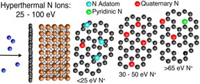 |
| Image: Schematic displaying the HyTII process depicting nitrogen (N+) incident with a graphene-on-copper (Cu) sample. The three-graphene flake schematics depict the type of modification resulting from N-HyTII processing over the labeled energy range.
CREDIT: US Naval Research Laboratory |
Abstract:
An interdisciplinary team of scientists at the U.S. Naval Research Laboratory (NRL), Electronics Science and Technology and Materials Science and Technology Divisions, has demonstrated hyperthermal ion implantation (HyTII) as an effective means of substitutionally doping graphene -- a hexagonally-arranged single-atomic thickness carbon sheet -- with nitrogen atoms. The result is a low-defect film with a tunable bandstructure amenable to a variety of device platforms and applications.
NRL develops new low-defect method to nitrogen dope graphene resulting in tunable bandstructure
Washington, DC | Posted on June 6th, 2016The research shows that the HyTII method delivers a high degree of control including doping concentration and, for the first time, demonstrates depth control of implantation by doping a single monolayer of graphene in a bilayer graphene stack. This further demonstrates that the resulting films have high-quality electronic transport properties that can be described solely by changes in bandstructure rather than the defect-dominated behavior of graphene films doped or functionalized using other methods.
"Since the discovery that a single atomic layer of sp2 bonded carbon atoms, termed graphene, could be isolated from bulk graphite, a plethora of remarkable electronic and spintronic properties have emerged," said Dr. Cory Cress, materials research engineer, NRL. "However, few applications are forthcoming because graphene lacks a bandgap and its doping is difficult to control, rendering graphene devices competitive only for highly-specialized device technologies."
Doping or chemical functionalization may add a usable transport gap. However, these methods tend to produce films that are plagued by unintentional defects, have low stability, or non-uniform coverage of dopants and functional groups, which all greatly limit their usefulness and degrade the intrinsic desirable properties of the graphene film.
As an alternative, NRL scientists leveraged their radiation-effects background to develop a hyperthermal ion implantation system with the necessary precision and control to implant nitrogen (N+) into graphene achieving doping via direct substitution.
"After many months of developing the system, the feasibility of the technique really depended on the first experiment," Cress said. "In our study, we determined the range of hyperthermal ion energies that yielded the highest fraction of nitrogen doping, while minimizing defects, and we were successful in confirming the inherent depth control of the HyTII process."
To achieve the latter, the scientists implemented a bilayer graphene material system comprising a layer of natural graphene, with mostly carbon-12 (12C) atoms, layered on graphene synthesized with greater than 99 percent carbon-13 (13C). This bilayer material provided a means to identify which layer they were modifying when analyzed with Raman spectroscopy.
Devices made from films processed with N+ in the range of optimal doping show a transition from strong to weak localization that depends on implantation dose, indicating the implanted nitrogen's ability to alter the intrinsic properties of the film. As further evidenced by the high electronic quality of the implanted devices over similar adatom-doped devices, the scientists found that the temperature dependence can be fit by a model that takes into account both band effects due to the substitutional doping and insulator-like effects due to defect formation, with the band effects observed to be the dominant component.
Surprisingly, the researchers found that a higher amount of nitrogen doping prevents the crossover to insulating behavior near the charge neutrality point. Defects appear to dominate the behavior only at large implantation energies, where defects are more probable, further demonstrating the differences between true-doped films and previous defective/doped films.
"Our measurements of these devices strongly indicate that we have finally fabricated a graphene film with a tunable bandgap, low defect density, and high stability," explains Dr. Adam L. Friedman, research physicist, NRL. "We therefore hypothesize that HyTII graphene films have great potential for electronic or spintronic applications for high-quality graphene where a transport or bandgap and high carrier concentration are desired."
###
The results of this research are reported in ACS Nano 10, 3714-3722 (2016), which details the fabrication method and efficient doping energy range, and Physical Review B: Rapid Communications 93, 161409(R) (2016), which details the electronic transport properties of devices made from the films. The researchers contributing to the ACS Nano paper include: Dr. Cory D. Cress; Dr. James C. Culbertson; and Dr. Jeremy T. Robinson of the Electronics Science and Technology Division; Dr. Adam L. Friedman of the Materials Science and Technology Division; Dr. Scott W. Schmucker and Dr. Pratibha Dev working at NRL as NRC Research Associates; and Dr. Joseph W. Lyding of the University of Illinois at Urbana-Champaign. The researchers contributing to the Phys. Rev. B: Rap. Comm. paper include: Dr. Adam L. Friedman and Dr. Olaf M.J. van 't Erve of the Materials Science and Technology Division; Dr. Cory D. Cress and Dr. Jeremy T. Robinson of the Electronics Science and Technology Division; and Dr. Scott W. Schmucker working at NRL as an NRC Research Associate.
####
For more information, please click here
Contacts:
Daniel Parry
202-767-2326
Copyright © Naval Research Laboratory
If you have a comment, please Contact us.Issuers of news releases, not 7th Wave, Inc. or Nanotechnology Now, are solely responsible for the accuracy of the content.
Bookmark:


| Related News Press |
News and information
![]() Quantum computer improves AI predictions April 17th, 2026
Quantum computer improves AI predictions April 17th, 2026
![]() Flexible sensor gains sensitivity under pressure April 17th, 2026
Flexible sensor gains sensitivity under pressure April 17th, 2026
![]() A reusable chip for particulate matter sensing April 17th, 2026
A reusable chip for particulate matter sensing April 17th, 2026
![]() Detecting vibrational quantum beating in the predissociation dynamics of SF6 using time-resolved photoelectron spectroscopy April 17th, 2026
Detecting vibrational quantum beating in the predissociation dynamics of SF6 using time-resolved photoelectron spectroscopy April 17th, 2026
Thin films
![]() Tiny nanosheets, big leap: A new sensor detects ethanol at ultra-low levels January 30th, 2026
Tiny nanosheets, big leap: A new sensor detects ethanol at ultra-low levels January 30th, 2026
Graphene/ Graphite
![]() Electrifying results shed light on graphene foam as a potential material for lab grown cartilage June 6th, 2025
Electrifying results shed light on graphene foam as a potential material for lab grown cartilage June 6th, 2025
![]() Breakthrough in proton barrier films using pore-free graphene oxide: Kumamoto University researchers achieve new milestone in advanced coating technologies September 13th, 2024
Breakthrough in proton barrier films using pore-free graphene oxide: Kumamoto University researchers achieve new milestone in advanced coating technologies September 13th, 2024
Govt.-Legislation/Regulation/Funding/Policy
![]() Quantum computer improves AI predictions April 17th, 2026
Quantum computer improves AI predictions April 17th, 2026
![]() Metasurfaces smooth light to boost magnetic sensing precision January 30th, 2026
Metasurfaces smooth light to boost magnetic sensing precision January 30th, 2026
![]() New imaging approach transforms study of bacterial biofilms August 8th, 2025
New imaging approach transforms study of bacterial biofilms August 8th, 2025
Possible Futures
![]() A fundamentally new therapeutic approach to cystic fibrosis: Nanobody repairs cellular defect April 17th, 2026
A fundamentally new therapeutic approach to cystic fibrosis: Nanobody repairs cellular defect April 17th, 2026
![]() UC Irvine physicists discover method to reverse �quantum scrambling� : The work addresses the problem of information loss in quantum computing system April 17th, 2026
UC Irvine physicists discover method to reverse �quantum scrambling� : The work addresses the problem of information loss in quantum computing system April 17th, 2026
Chip Technology
![]() A reusable chip for particulate matter sensing April 17th, 2026
A reusable chip for particulate matter sensing April 17th, 2026
![]() Metasurfaces smooth light to boost magnetic sensing precision January 30th, 2026
Metasurfaces smooth light to boost magnetic sensing precision January 30th, 2026
Nanoelectronics
![]() Lab to industry: InSe wafer-scale breakthrough for future electronics August 8th, 2025
Lab to industry: InSe wafer-scale breakthrough for future electronics August 8th, 2025
![]() Interdisciplinary: Rice team tackles the future of semiconductors Multiferroics could be the key to ultralow-energy computing October 6th, 2023
Interdisciplinary: Rice team tackles the future of semiconductors Multiferroics could be the key to ultralow-energy computing October 6th, 2023
![]() Key element for a scalable quantum computer: Physicists from Forschungszentrum J�lich and RWTH Aachen University demonstrate electron transport on a quantum chip September 23rd, 2022
Key element for a scalable quantum computer: Physicists from Forschungszentrum J�lich and RWTH Aachen University demonstrate electron transport on a quantum chip September 23rd, 2022
![]() Reduced power consumption in semiconductor devices September 23rd, 2022
Reduced power consumption in semiconductor devices September 23rd, 2022
Discoveries
![]() Quantum computer improves AI predictions April 17th, 2026
Quantum computer improves AI predictions April 17th, 2026
![]() Flexible sensor gains sensitivity under pressure April 17th, 2026
Flexible sensor gains sensitivity under pressure April 17th, 2026
![]() A reusable chip for particulate matter sensing April 17th, 2026
A reusable chip for particulate matter sensing April 17th, 2026
![]() Detecting vibrational quantum beating in the predissociation dynamics of SF6 using time-resolved photoelectron spectroscopy April 17th, 2026
Detecting vibrational quantum beating in the predissociation dynamics of SF6 using time-resolved photoelectron spectroscopy April 17th, 2026
Materials/Metamaterials/Magnetoresistance
![]() First real-time observation of two-dimensional melting process: Researchers at Mainz University unveil new insights into magnetic vortex structures August 8th, 2025
First real-time observation of two-dimensional melting process: Researchers at Mainz University unveil new insights into magnetic vortex structures August 8th, 2025
![]() Researchers unveil a groundbreaking clay-based solution to capture carbon dioxide and combat climate change June 6th, 2025
Researchers unveil a groundbreaking clay-based solution to capture carbon dioxide and combat climate change June 6th, 2025
![]() A 1960s idea inspires NBI researchers to study hitherto inaccessible quantum states June 6th, 2025
A 1960s idea inspires NBI researchers to study hitherto inaccessible quantum states June 6th, 2025
![]() Institute for Nanoscience hosts annual proposal planning meeting May 16th, 2025
Institute for Nanoscience hosts annual proposal planning meeting May 16th, 2025
Announcements
![]() A fundamentally new therapeutic approach to cystic fibrosis: Nanobody repairs cellular defect April 17th, 2026
A fundamentally new therapeutic approach to cystic fibrosis: Nanobody repairs cellular defect April 17th, 2026
![]() UC Irvine physicists discover method to reverse �quantum scrambling� : The work addresses the problem of information loss in quantum computing system April 17th, 2026
UC Irvine physicists discover method to reverse �quantum scrambling� : The work addresses the problem of information loss in quantum computing system April 17th, 2026
Interviews/Book Reviews/Essays/Reports/Podcasts/Journals/White papers/Posters
![]() A fundamentally new therapeutic approach to cystic fibrosis: Nanobody repairs cellular defect April 17th, 2026
A fundamentally new therapeutic approach to cystic fibrosis: Nanobody repairs cellular defect April 17th, 2026
![]() UC Irvine physicists discover method to reverse �quantum scrambling� : The work addresses the problem of information loss in quantum computing system April 17th, 2026
UC Irvine physicists discover method to reverse �quantum scrambling� : The work addresses the problem of information loss in quantum computing system April 17th, 2026
Research partnerships
![]() Lab to industry: InSe wafer-scale breakthrough for future electronics August 8th, 2025
Lab to industry: InSe wafer-scale breakthrough for future electronics August 8th, 2025
![]() HKU physicists uncover hidden order in the quantum world through deconfined quantum critical points April 25th, 2025
HKU physicists uncover hidden order in the quantum world through deconfined quantum critical points April 25th, 2025
|
|
||
|
|
||
| The latest news from around the world, FREE | ||
|
|
||
|
|
||
| Premium Products | ||
|
|
||
|
Only the news you want to read!
Learn More |
||
|
|
||
|
Full-service, expert consulting
Learn More |
||
|
|
||