Home > Press > Graphene: Progress, not quantum leaps
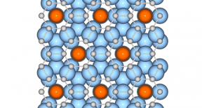 |
| The interactions between graphene and its environment have a significant influence on the use of this promising material by the semiconductor industry. Thanks to the comprehensive findings of an international research project, these interactions are now better understood and can be controlled as a result. Credit: Austrian Science Fund (FWF) |
Abstract:
The interactions between graphene and its environment have a significant influence on the use of this promising material by the semiconductor industry. Thanks to the comprehensive findings of an international research project, these interactions are now better understood and can be controlled as a result.
Graphene: Progress, not quantum leaps
Vienna, Austria | Posted on May 23rd, 2016Graphene is an atom-thin layer of carbon. Thanks to its unique structural and electronic characteristics, the material has enormous potential and has been the focus of many high expectations � however, concrete uses and applications have yet to materialise. As is so often the case when it comes to viable application, the devil is in the detail. A project funded by the Austrian Science Fund FWF has managed to come to grips with some of these "devils".
TARGETING SEMICONDUCTORS
"Individual components based on graphene already present outstanding characteristics", explains project leader Thomas Pichler from the Electronic Properties of Materials Department at the University of Vienna. "However, the major breakthrough in its application as an integrated electronic component has not yet emerged. It has simply not been possible to use this material for established semiconductor technology in a way that can be reliably replicated." One of the biggest obstacles up to now was the lack of control of how graphene interacts with its environment at atomic level. As a result, it has been almost impossible to deploy the material in a predictable and targeted way up to now. Even the interaction between graphene and the substrate, to which it must be applied due to its extreme thinness, was only understood in part. Pichler and his research team have succeeded in changing exactly this.
STRAIN WITH CHARGE
The team was also immediately successful in gaining some surprising new insights. "We were able to demonstrate a correlation between charge transfer � the shifting of electrons � and mechanical strain in graphene for the first time", says Pichler, explaining one outstanding result of the recently concluded project. "This observation could be of major practical significance, as it means that the entirely contactless measurement of internal strain in graphene-based components may be possible in the future." The team also achieved significant successes in the targeted control of the environment of graphene: within the framework of the project it was possible to control the interface between graphene and traditional semiconductors like germanium on the atomic level for the first time. Many view this as an important step towards making graphene-based nanoelectronic components usable for semiconductor technology.
SUCCESS WITH METHOD
Crucial to the success of the cooperative project was its optimal combination and implementation of two methodically different processes. Pichler and his team therefore used the very latest spectroscopy measurement techniques and complemented them with so-called ab-initio calculations, which were carried out by a team headed by Ludger Wirtz from the Institute for Electronics, Microelectronics and Nanotechnology at the University of Lille.
EXTENSIVE SAMPLES
The second secret of the project's success was the fact that it succeeded in producing extensive samples of electronically insulated graphene. This provided an optimal starting material for the experimental work. "We then deliberately manipulated the electronic structure of the graphene", says Pichler, explaining the approach adopted by the project. "To do this, for example, we replaced certain atoms in the graphene substrate with hydrogen or nitrogen atoms and measured the impact of this substitution on the graphene." Another approach adopted by Pichler and his team involved a method known as intercalation. With this method, wafer-thin layers of potassium, lithium or barium are inserted between the graphene and the substrate and the resulting impact on the graphene is characterised.
These steps paved the way for many other advances arising from the FWF project, which are still needed to enable the comprehensive use of the miracle material graphene. Many challenges remain to be overcome before a "miracle-worker" like graphene can be put to practical use. Basic research will play a key role in overcoming these challenges.
Personal details
Thomas Pichler is Head of the "Electronic Properties of Materials" (epm.univie.ac.at/electronic-properties-of-materials/) research group at the Faculty of Physics (physik.univie.ac.at/en/home/) of the University of Vienna (www.univie.ac.at/?L=2). He is an expert in the control of the electronic and optical properties of quantum solids like nanotubes and graphene. Prior to taking up the professorship in Vienna, he was Head of the "Molecular Nanostructures" group at the Leibniz Institute for Solid State and Materials Research ( https://www.ifw-dresden.de/en/ ) in Dresden, Germany.
####
For more information, please click here
Contacts:
Scientific Contact:
Prof. Thomas Pichler
University of Vienna
Faculty of Physics
Boltzmanngasse 5
1090 Vienna, Austria
M +43 / 664 / 60277 - 51466
W http://www.univie.ac.at/en
Austrian Science Fund FWF:
Marc Seumenicht
Haus der Forschung
Sensengasse 1
1090 Vienna, Austria
T +43 / 1 / 505 67 40 - 8111
W http://www.fwf.ac.at/en
Copy Editing and Distribution:
PR&D � Public Relations for Research & Education
Mariannengasse 8
1090 Vienna, Austria
T +43 / 1 / 505 70 44
W http://www.prd.at/en
Copyright © University of Vienna
If you have a comment, please Contact us.Issuers of news releases, not 7th Wave, Inc. or Nanotechnology Now, are solely responsible for the accuracy of the content.
Bookmark:


| Related Links |
| Related News Press |
News and information
![]() Quantum computer improves AI predictions April 17th, 2026
Quantum computer improves AI predictions April 17th, 2026
![]() Flexible sensor gains sensitivity under pressure April 17th, 2026
Flexible sensor gains sensitivity under pressure April 17th, 2026
![]() A reusable chip for particulate matter sensing April 17th, 2026
A reusable chip for particulate matter sensing April 17th, 2026
![]() Detecting vibrational quantum beating in the predissociation dynamics of SF6 using time-resolved photoelectron spectroscopy April 17th, 2026
Detecting vibrational quantum beating in the predissociation dynamics of SF6 using time-resolved photoelectron spectroscopy April 17th, 2026
Graphene/ Graphite
![]() Electrifying results shed light on graphene foam as a potential material for lab grown cartilage June 6th, 2025
Electrifying results shed light on graphene foam as a potential material for lab grown cartilage June 6th, 2025
![]() Breakthrough in proton barrier films using pore-free graphene oxide: Kumamoto University researchers achieve new milestone in advanced coating technologies September 13th, 2024
Breakthrough in proton barrier films using pore-free graphene oxide: Kumamoto University researchers achieve new milestone in advanced coating technologies September 13th, 2024
Possible Futures
![]() A fundamentally new therapeutic approach to cystic fibrosis: Nanobody repairs cellular defect April 17th, 2026
A fundamentally new therapeutic approach to cystic fibrosis: Nanobody repairs cellular defect April 17th, 2026
![]() UC Irvine physicists discover method to reverse �quantum scrambling� : The work addresses the problem of information loss in quantum computing system April 17th, 2026
UC Irvine physicists discover method to reverse �quantum scrambling� : The work addresses the problem of information loss in quantum computing system April 17th, 2026
Academic/Education
![]() Rice University launches Rice Synthetic Biology Institute to improve lives January 12th, 2024
Rice University launches Rice Synthetic Biology Institute to improve lives January 12th, 2024
![]() Multi-institution, $4.6 million NSF grant to fund nanotechnology training September 9th, 2022
Multi-institution, $4.6 million NSF grant to fund nanotechnology training September 9th, 2022
Chip Technology
![]() A reusable chip for particulate matter sensing April 17th, 2026
A reusable chip for particulate matter sensing April 17th, 2026
![]() Metasurfaces smooth light to boost magnetic sensing precision January 30th, 2026
Metasurfaces smooth light to boost magnetic sensing precision January 30th, 2026
Discoveries
![]() Quantum computer improves AI predictions April 17th, 2026
Quantum computer improves AI predictions April 17th, 2026
![]() Flexible sensor gains sensitivity under pressure April 17th, 2026
Flexible sensor gains sensitivity under pressure April 17th, 2026
![]() A reusable chip for particulate matter sensing April 17th, 2026
A reusable chip for particulate matter sensing April 17th, 2026
![]() Detecting vibrational quantum beating in the predissociation dynamics of SF6 using time-resolved photoelectron spectroscopy April 17th, 2026
Detecting vibrational quantum beating in the predissociation dynamics of SF6 using time-resolved photoelectron spectroscopy April 17th, 2026
Materials/Metamaterials/Magnetoresistance
![]() First real-time observation of two-dimensional melting process: Researchers at Mainz University unveil new insights into magnetic vortex structures August 8th, 2025
First real-time observation of two-dimensional melting process: Researchers at Mainz University unveil new insights into magnetic vortex structures August 8th, 2025
![]() Researchers unveil a groundbreaking clay-based solution to capture carbon dioxide and combat climate change June 6th, 2025
Researchers unveil a groundbreaking clay-based solution to capture carbon dioxide and combat climate change June 6th, 2025
![]() A 1960s idea inspires NBI researchers to study hitherto inaccessible quantum states June 6th, 2025
A 1960s idea inspires NBI researchers to study hitherto inaccessible quantum states June 6th, 2025
![]() Institute for Nanoscience hosts annual proposal planning meeting May 16th, 2025
Institute for Nanoscience hosts annual proposal planning meeting May 16th, 2025
Announcements
![]() A fundamentally new therapeutic approach to cystic fibrosis: Nanobody repairs cellular defect April 17th, 2026
A fundamentally new therapeutic approach to cystic fibrosis: Nanobody repairs cellular defect April 17th, 2026
![]() UC Irvine physicists discover method to reverse �quantum scrambling� : The work addresses the problem of information loss in quantum computing system April 17th, 2026
UC Irvine physicists discover method to reverse �quantum scrambling� : The work addresses the problem of information loss in quantum computing system April 17th, 2026
Interviews/Book Reviews/Essays/Reports/Podcasts/Journals/White papers/Posters
![]() A fundamentally new therapeutic approach to cystic fibrosis: Nanobody repairs cellular defect April 17th, 2026
A fundamentally new therapeutic approach to cystic fibrosis: Nanobody repairs cellular defect April 17th, 2026
![]() UC Irvine physicists discover method to reverse �quantum scrambling� : The work addresses the problem of information loss in quantum computing system April 17th, 2026
UC Irvine physicists discover method to reverse �quantum scrambling� : The work addresses the problem of information loss in quantum computing system April 17th, 2026
|
|
||
|
|
||
| The latest news from around the world, FREE | ||
|
|
||
|
|
||
| Premium Products | ||
|
|
||
|
Only the news you want to read!
Learn More |
||
|
|
||
|
Full-service, expert consulting
Learn More |
||
|
|
||