Home > Press > Bruker Introduces First of Its Kind Dimensional Analysis System: The Novel Contour CMM™ System Fully Integrates 3D Coordinate Measurements with Nanoscale Surface Height, Texture, Waviness and Form Characterization
 |
Abstract:
At the 30th Control International (www.control-messe.de) trade fair for quality assurance, Bruker (NASDAQ: BRKR) today announced the release of the innovative and unique Contour CMM™ dimensional analysis system, which is the world’s first non-contact metrology system to perform simultaneous nanoscale surface height, texture, waviness and form measurements, as well as 3D coordinate measurements for geometric dimensioning and tolerancing (GD&T), all on one instrument. Leveraging decades of world-leading optical metrology innovation, the system performs rapid, non-contact precision measurements to meet the industry’s most stringent standards. The Contour CMM system enables more accurate and convenient metrology for R&D and manufacturing of small structures in precision-machined components across a wide range of industries, from medical devices and optics, to automotive and aerospace.
Bruker Introduces First of Its Kind Dimensional Analysis System: The Novel Contour CMM™ System Fully Integrates 3D Coordinate Measurements with Nanoscale Surface Height, Texture, Waviness and Form Characterization
Stuttgart, Germany | Posted on April 26th, 2016“Contour CMM is an exciting breakthrough in the marriage of high-resolution optical surface profiling and coordinate measurement,” said Donald K. Cohen, Ph.D., Managing Member at Michigan Metrology, LLC. “It will allow engineers and researchers to examine parts in a completely new way and develop data that has previously been impossible to generate. Designers and manufacturers of precision components will gain significant value from having this capability to accelerate development and increase the quality of their products.”
“The Contour CMM system is a new enabler that fills a technology gap that industry has desired to bridge for many years,” added James Earle, Vice President and General Manager of Bruker’s Tribology, Stylus and Optical Metrology Business. “Our customers have had to face the uncertainties that come from fusing data from multiple technologies to solve manufacturing problems or investigate materials. Now they can get all the detailed surface metrology they have come to rely upon from our systems, and also locate that data within the larger form for true, one-stop characterization.”
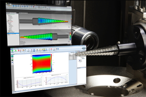
About the Contour CMM Dimensional Analysis System
Contour CMM transcends the boundaries of surface and coordinate characterization, quantifying a metrology continuum from surface roughness and texture through waviness into true 3D coordinate measurements of geometric dimensions with tolerancing analysis. The instrument exploits Bruker’s industry-leading Wyko® interferometric optical profiling technology in a proprietary optical probe. This generates extremely high vertical (2-nanometer) and lateral (0.9 micron) resolution surface finish data. High accuracy stages enable utilization of this surface data as building blocks for a true part coordinate system with form error less than 2 microns. Its Vision Dimensions™ software offers proprietary features specifically designed for small-part characterization, including automation for part programs, hundreds of preset analyses, and customized inspection reports. For advanced R&D, such as the measurement of material wear on medical implants or bearing races, the Contour CMM system provides, in a single instrument, the ability to quantify the smallest of wear scars with submicron accuracy, while enabling engineers to position where the scars are on the parts and report the deviation of the inspected part from CAD.
####
About Bruker Nano Surfaces Division
For more than 50 years, Bruker has enabled scientists to make breakthrough discoveries and develop new applications that improve the quality of human life. Bruker’s high-performance, scientific research instruments and high-value analytical solutions enable scientists to explore life and materials at molecular, cellular and microscopic levels.
In close cooperation with our customers, Bruker is enabling innovation, productivity and customer success in life science molecular research, in applied and pharma applications, in microscopy, nano-analysis and industrial applications, as well as in cell biology, preclinical imaging, clinical research, microbiology and molecular diagnostics.
For more information, please click here
Contacts:
Stephen Hopkins
Marketing Communications
Bruker Nano Surfaces Division
T: +1 (520) 741-1044 x1022
Copyright © Bruker Nano Surfaces Division
If you have a comment, please Contact us.Issuers of news releases, not 7th Wave, Inc. or Nanotechnology Now, are solely responsible for the accuracy of the content.
Bookmark:


| Related News Press |
News and information
![]() Quantum computer improves AI predictions April 17th, 2026
Quantum computer improves AI predictions April 17th, 2026
![]() Flexible sensor gains sensitivity under pressure April 17th, 2026
Flexible sensor gains sensitivity under pressure April 17th, 2026
![]() A reusable chip for particulate matter sensing April 17th, 2026
A reusable chip for particulate matter sensing April 17th, 2026
![]() Detecting vibrational quantum beating in the predissociation dynamics of SF6 using time-resolved photoelectron spectroscopy April 17th, 2026
Detecting vibrational quantum beating in the predissociation dynamics of SF6 using time-resolved photoelectron spectroscopy April 17th, 2026
Imaging
![]() Simple algorithm paired with standard imaging tool could predict failure in lithium metal batteries August 8th, 2025
Simple algorithm paired with standard imaging tool could predict failure in lithium metal batteries August 8th, 2025
Announcements
![]() A fundamentally new therapeutic approach to cystic fibrosis: Nanobody repairs cellular defect April 17th, 2026
A fundamentally new therapeutic approach to cystic fibrosis: Nanobody repairs cellular defect April 17th, 2026
![]() UC Irvine physicists discover method to reverse ‘quantum scrambling’ : The work addresses the problem of information loss in quantum computing system April 17th, 2026
UC Irvine physicists discover method to reverse ‘quantum scrambling’ : The work addresses the problem of information loss in quantum computing system April 17th, 2026
Tools
![]() Metasurfaces smooth light to boost magnetic sensing precision January 30th, 2026
Metasurfaces smooth light to boost magnetic sensing precision January 30th, 2026
![]() From sensors to smart systems: the rise of AI-driven photonic noses January 30th, 2026
From sensors to smart systems: the rise of AI-driven photonic noses January 30th, 2026
![]() Japan launches fully domestically produced quantum computer: Expo visitors to experience quantum computing firsthand August 8th, 2025
Japan launches fully domestically produced quantum computer: Expo visitors to experience quantum computing firsthand August 8th, 2025
|
|
||
|
|
||
| The latest news from around the world, FREE | ||
|
|
||
|
|
||
| Premium Products | ||
|
|
||
|
Only the news you want to read!
Learn More |
||
|
|
||
|
Full-service, expert consulting
Learn More |
||
|
|
||