Home > Press > Effective graphene doping depends on substrate material
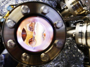 |
| Sample imaged using ARPES: Scientists at PGI-3 used angle-resolved photoelectron spectroscopy (ARPES) to determine the degree of doping in the graphene samples. For this method, the samples are irradiated with UV light to detach electrons from the materials. The electrons can then be detected. The original bond energy of the detached electrons determines the velocity at which they hit the detector. In this way, the scientists were able to reconstruct the band structure of the graphene.
Copyright: Forschungszentrum Juelich |
Abstract:
Juelich physicists have discovered unexpected effects in doped graphene - i.e. graphene that is mixed with foreign atoms. They investigated samples of the carbon compound enriched with the foreign atom nitrogen on various substrate materials. Unwanted interactions with these substrates can influence the electric properties of graphene. The researchers at the Peter Gruenberg Institute have now shown that effective doping depends on the choice of substrate material. The scientists' results were published in the journal Physical Review Letters.
Effective graphene doping depends on substrate material
Juelich, Germany | Posted on March 30th, 2016Harder than diamond and tougher than steel, light weight, transparent, flexible, and extremely conductive: the mesh material graphene is regarded as the material of the future. It could make computers faster, mobile phones more flexible, and touchscreens thinner. But so far, the industrial production of the carbon lattice, which is only one atom thick, has proven problematic: in almost all cases, a substrate is required. The search for a suitable material for this purpose is one of the major challenges on the path towards practical applications because if undesirable interactions occur, they can cause the graphene to lose its electric properties.
For some years, scientists have been testing silicon carbide - a crystalline compound of silicon and carbon - for its suitability as a substrate material. When the material is heated to more than 1400 degrees Celsius in an argon atmosphere, graphene can be grown on the crystal. However, this 'epitaxial monolayer graphene' displays - very slight - interaction with the substrate, which limits its electron mobility.
In order to circumvent this problem, hydrogen is introduced into the interface between the two materials. This method is known as hydrogen intercalation. The bonds between the graphene and the substrate material are separated and saturated by the hydrogen atoms. This suppresses the electronic influence of the silicon crystal while the graphene stays mechanically joined with the substrate: quasi-free-standing monolayer graphene.
High-precision measurements with standing X-rays
For practical applications, the electrical properties of graphene must be modifiable - for example by introducing additional electrons into the material. This is effected by targeted "contamination" of the carbon lattice with foreign atoms. For this process, known as doping, the graphene is bombarded with nitrogen ions and then annealed. This results in defects in the lattice structure: some few carbon atoms - fewer than 1 % - separate from the lattice and are replaced with nitrogen atoms, which bring along additional electrons.
Scientists at Juelich's Peter Gruenberg Institute - Functional Nanostructures at Surfaces (PGI-3) have now, for the first time, studied whether and how the structure of the substrate material influences this doping process. At the synchrotron radiation source Diamond Light Source in Didcot, Oxfordshire, UK, Francois C. Bocquet and his colleagues doped samples of epitaxial and quasi-free-standing monolayer graphene and investigated its structural and electronic properties. By means of standing X-ray wave fields, they were able to scan both graphene and substrate at a precision of a few millionths of a micrometre - less than a tenth of the radius of an atom.
Nitrogen atoms in the interface layer are also suitable for doping
Their findings were surprising. "Some of the nitrogen atoms diffused from the graphene into the silicon carbide," explains Bocquet. "It was previously believed that the nitrogen bombardment only affected the graphene, but not the substrate material."
Although both samples were treated in the same way, they exhibited different nitrogen concentrations, but almost identical electronic doping: not all nitrogen atoms were integrated in the graphene lattice, nevertheless the number of electrons in the graphene rose as if this were the case. The key to this unexpected result lies in the different behaviour of the interface layers between graphene and substrate. For the epitaxial graphene, nothing changed: the interface layer remained stable, the structure unchanged. In the quasi-free-standing graphene, however, some of the hydrogen atoms between graphene and substrate were replaced with nitrogen atoms. According to Bocquet: "If you examine the quasi-free-standing graphene, you will find a nitrogen atom underneath the graphene coat in some places. These nitrogen atoms, although they are not part of the graphene, can dope the lattice without destroying it. This unforeseen result is very promising for future applications in micro- and nanoelectronics."
####
For more information, please click here
Contacts:
Regine Panknin
49-246-161-9054
Copyright © Forschungszentrum Juelich
If you have a comment, please Contact us.Issuers of news releases, not 7th Wave, Inc. or Nanotechnology Now, are solely responsible for the accuracy of the content.
Bookmark:


| Related Links |
| Related News Press |
News and information
![]() Quantum computer improves AI predictions April 17th, 2026
Quantum computer improves AI predictions April 17th, 2026
![]() Flexible sensor gains sensitivity under pressure April 17th, 2026
Flexible sensor gains sensitivity under pressure April 17th, 2026
![]() A reusable chip for particulate matter sensing April 17th, 2026
A reusable chip for particulate matter sensing April 17th, 2026
![]() Detecting vibrational quantum beating in the predissociation dynamics of SF6 using time-resolved photoelectron spectroscopy April 17th, 2026
Detecting vibrational quantum beating in the predissociation dynamics of SF6 using time-resolved photoelectron spectroscopy April 17th, 2026
Imaging
![]() Simple algorithm paired with standard imaging tool could predict failure in lithium metal batteries August 8th, 2025
Simple algorithm paired with standard imaging tool could predict failure in lithium metal batteries August 8th, 2025
Graphene/ Graphite
![]() Electrifying results shed light on graphene foam as a potential material for lab grown cartilage June 6th, 2025
Electrifying results shed light on graphene foam as a potential material for lab grown cartilage June 6th, 2025
![]() Breakthrough in proton barrier films using pore-free graphene oxide: Kumamoto University researchers achieve new milestone in advanced coating technologies September 13th, 2024
Breakthrough in proton barrier films using pore-free graphene oxide: Kumamoto University researchers achieve new milestone in advanced coating technologies September 13th, 2024
Possible Futures
![]() A fundamentally new therapeutic approach to cystic fibrosis: Nanobody repairs cellular defect April 17th, 2026
A fundamentally new therapeutic approach to cystic fibrosis: Nanobody repairs cellular defect April 17th, 2026
![]() UC Irvine physicists discover method to reverse �quantum scrambling� : The work addresses the problem of information loss in quantum computing system April 17th, 2026
UC Irvine physicists discover method to reverse �quantum scrambling� : The work addresses the problem of information loss in quantum computing system April 17th, 2026
Chip Technology
![]() A reusable chip for particulate matter sensing April 17th, 2026
A reusable chip for particulate matter sensing April 17th, 2026
![]() Metasurfaces smooth light to boost magnetic sensing precision January 30th, 2026
Metasurfaces smooth light to boost magnetic sensing precision January 30th, 2026
Nanoelectronics
![]() Lab to industry: InSe wafer-scale breakthrough for future electronics August 8th, 2025
Lab to industry: InSe wafer-scale breakthrough for future electronics August 8th, 2025
![]() Interdisciplinary: Rice team tackles the future of semiconductors Multiferroics could be the key to ultralow-energy computing October 6th, 2023
Interdisciplinary: Rice team tackles the future of semiconductors Multiferroics could be the key to ultralow-energy computing October 6th, 2023
![]() Key element for a scalable quantum computer: Physicists from Forschungszentrum J�lich and RWTH Aachen University demonstrate electron transport on a quantum chip September 23rd, 2022
Key element for a scalable quantum computer: Physicists from Forschungszentrum J�lich and RWTH Aachen University demonstrate electron transport on a quantum chip September 23rd, 2022
![]() Reduced power consumption in semiconductor devices September 23rd, 2022
Reduced power consumption in semiconductor devices September 23rd, 2022
Discoveries
![]() Quantum computer improves AI predictions April 17th, 2026
Quantum computer improves AI predictions April 17th, 2026
![]() Flexible sensor gains sensitivity under pressure April 17th, 2026
Flexible sensor gains sensitivity under pressure April 17th, 2026
![]() A reusable chip for particulate matter sensing April 17th, 2026
A reusable chip for particulate matter sensing April 17th, 2026
![]() Detecting vibrational quantum beating in the predissociation dynamics of SF6 using time-resolved photoelectron spectroscopy April 17th, 2026
Detecting vibrational quantum beating in the predissociation dynamics of SF6 using time-resolved photoelectron spectroscopy April 17th, 2026
Materials/Metamaterials/Magnetoresistance
![]() First real-time observation of two-dimensional melting process: Researchers at Mainz University unveil new insights into magnetic vortex structures August 8th, 2025
First real-time observation of two-dimensional melting process: Researchers at Mainz University unveil new insights into magnetic vortex structures August 8th, 2025
![]() Researchers unveil a groundbreaking clay-based solution to capture carbon dioxide and combat climate change June 6th, 2025
Researchers unveil a groundbreaking clay-based solution to capture carbon dioxide and combat climate change June 6th, 2025
![]() A 1960s idea inspires NBI researchers to study hitherto inaccessible quantum states June 6th, 2025
A 1960s idea inspires NBI researchers to study hitherto inaccessible quantum states June 6th, 2025
![]() Institute for Nanoscience hosts annual proposal planning meeting May 16th, 2025
Institute for Nanoscience hosts annual proposal planning meeting May 16th, 2025
Announcements
![]() A fundamentally new therapeutic approach to cystic fibrosis: Nanobody repairs cellular defect April 17th, 2026
A fundamentally new therapeutic approach to cystic fibrosis: Nanobody repairs cellular defect April 17th, 2026
![]() UC Irvine physicists discover method to reverse �quantum scrambling� : The work addresses the problem of information loss in quantum computing system April 17th, 2026
UC Irvine physicists discover method to reverse �quantum scrambling� : The work addresses the problem of information loss in quantum computing system April 17th, 2026
Interviews/Book Reviews/Essays/Reports/Podcasts/Journals/White papers/Posters
![]() A fundamentally new therapeutic approach to cystic fibrosis: Nanobody repairs cellular defect April 17th, 2026
A fundamentally new therapeutic approach to cystic fibrosis: Nanobody repairs cellular defect April 17th, 2026
![]() UC Irvine physicists discover method to reverse �quantum scrambling� : The work addresses the problem of information loss in quantum computing system April 17th, 2026
UC Irvine physicists discover method to reverse �quantum scrambling� : The work addresses the problem of information loss in quantum computing system April 17th, 2026
|
|
||
|
|
||
| The latest news from around the world, FREE | ||
|
|
||
|
|
||
| Premium Products | ||
|
|
||
|
Only the news you want to read!
Learn More |
||
|
|
||
|
Full-service, expert consulting
Learn More |
||
|
|
||