Home > Press > New way to control particle motions on 2-D materials
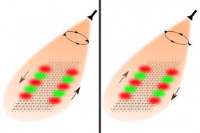 |
| Researchers used the spin of light to guide the flow of optical information. Shining right-circularly polarized light on nanoribbons made of special 2-D materials enables light to flow forward on one edge and backward on the other edge. Changing the polarization of the light causes the guided modes to reverse directions.
Image: Anshuman Kumar Srivastava |
Abstract:
Researchers at MIT and other institutions have found a new phenomenon in the behavior of a kind of quasiparticles called plasmons as they move along tiny ribbons of two-dimensional materials such as graphene and TMDs (transition metal dichalcogenides), which have a hexagonal structure resembling chicken wire. The team found that these plasmons can be separated into two different streams moving in opposite directions at the edges of the ribbons, like traffic on a two-lane highway, without the need for strong magnetic fields or other exotic conditions.
New way to control particle motions on 2-D materials
Cambridge, MA | Posted on March 22nd, 2016The new research was carried out by MIT associate professor of mechanical engineering Nicholas X. Fang, recent PhD graduate from that department Anshuman Kumar, and four other researchers from the University of Wisconsin at Milwaukee, Hong Kong Polytechnic University, and the University of Minnesota. The work was reported in a paper in the journal Physical Review B.
Other groups had previously observed such separated flows, Fang says, but that previous work required the use of powerful magnetic fields. Instead, the new process relies largely on optical effects, he says, using beams of circularly polarized light.
The findings are based on exotic states of matter that can occur in two-dimensional materials that, unlike graphene, have a characteristic known as a bandgap, necessary for devices such as transistors or solar cells (and also in graphene that is modified to have a bandgap). These states of matter are based on quantum physics phenomena such as Berry curvature, which occur in configurations known as massive Dirac systems. Although such systems are a hot area of research these days, the researchers say this particular class of phenomena, involving surface electromagnetic properties known as surface plasmons, has been relatively unexplored until now.
Clustering in "valleys"
In the new work, the team showed that shining beams of circularly polarized light onto the graphene ribbons causes electrons in the material to cluster into two different "valleys" in the electronic band structure. The peculiar symmetry properties of this system gives rise to a phenomenon called Berry curvature, which can be thought of as an artificial magnetic field.
Under these conditions, these valleys correspond to motions of the plasmons -- which are a kind of oscillation of electron density in the material -- in opposite directions on the two edges of the material. The graphene ribbons are just 50 nanometers (billionths of a meter) in width.
This effective magnetic field can be measured by sending in a second polarized beam, whose transmission can then be detected so that the changes in its polarization give a direct measurement of the effects taking place in the surface plasmons.
"This is exciting," Fang explains, because it opens up a whole new approach to both manipulating the electromagnetic behavior of such systems and measuring the results of these manipulations.
This could suggest possibilities for new kinds of electro-optical devices, he says. For example, some experimental photonic systems require devices called optical isolators, which prevent beams of light in precision optical systems from being reflected back to their source and causing interference. But these isolators, which require strong magnetic fields, are inherently bulky, he says, limiting the usefulness of such systems. "With this concept," he says, "it's possible to replace these bulky optical isolators with one monolayer of two-dimensional material."
Chip-scale isolation
With such a system, Kumar says, it should be possible "to do chip-scale optical isolation without the need for a magnetic field." To achieve the same degree of optical isolation that this system would provide with a beam of light, Kumar says, with a conventional system would require a magnetic field with a strength of 7 tesla -- a very strong field that would require a special research facility. (By comparison, the Earth's magnetic field measures just 32 millionths of a tesla).
Theoretically, this could lead to applications such as new types of memory devices where information could be both written and read by using beams of polarized light, making them relatively immune to electromagnetic or other kinds of interference, the researchers say.
###
In addition to Fang and Kumar, the team included Andrei Nemilentsau and George Hanson at the University of Wisconsin at Madison, Kin Hung Fung at Hong Kong Polytechnic University, and Tony Low at the University of Minnesota. The work was supported by the National Science Foundation and the Air Force Office of Scientific Research.
####
For more information, please click here
Contacts:
Sarah McDonnell
617-253-8923
Copyright © Massachusetts Institute of Technology
If you have a comment, please Contact us.Issuers of news releases, not 7th Wave, Inc. or Nanotechnology Now, are solely responsible for the accuracy of the content.
Bookmark:


| Related News Press |
News and information
![]() Quantum computer improves AI predictions April 17th, 2026
Quantum computer improves AI predictions April 17th, 2026
![]() Flexible sensor gains sensitivity under pressure April 17th, 2026
Flexible sensor gains sensitivity under pressure April 17th, 2026
![]() A reusable chip for particulate matter sensing April 17th, 2026
A reusable chip for particulate matter sensing April 17th, 2026
![]() Detecting vibrational quantum beating in the predissociation dynamics of SF6 using time-resolved photoelectron spectroscopy April 17th, 2026
Detecting vibrational quantum beating in the predissociation dynamics of SF6 using time-resolved photoelectron spectroscopy April 17th, 2026
Graphene/ Graphite
![]() Electrifying results shed light on graphene foam as a potential material for lab grown cartilage June 6th, 2025
Electrifying results shed light on graphene foam as a potential material for lab grown cartilage June 6th, 2025
![]() Breakthrough in proton barrier films using pore-free graphene oxide: Kumamoto University researchers achieve new milestone in advanced coating technologies September 13th, 2024
Breakthrough in proton barrier films using pore-free graphene oxide: Kumamoto University researchers achieve new milestone in advanced coating technologies September 13th, 2024
Possible Futures
![]() A fundamentally new therapeutic approach to cystic fibrosis: Nanobody repairs cellular defect April 17th, 2026
A fundamentally new therapeutic approach to cystic fibrosis: Nanobody repairs cellular defect April 17th, 2026
![]() UC Irvine physicists discover method to reverse �quantum scrambling� : The work addresses the problem of information loss in quantum computing system April 17th, 2026
UC Irvine physicists discover method to reverse �quantum scrambling� : The work addresses the problem of information loss in quantum computing system April 17th, 2026
Chip Technology
![]() A reusable chip for particulate matter sensing April 17th, 2026
A reusable chip for particulate matter sensing April 17th, 2026
![]() Metasurfaces smooth light to boost magnetic sensing precision January 30th, 2026
Metasurfaces smooth light to boost magnetic sensing precision January 30th, 2026
Optical computing/Photonic computing
![]() ICFO researchers overcome long-standing bottleneck in single photon detection with twisted 2D materials August 8th, 2025
ICFO researchers overcome long-standing bottleneck in single photon detection with twisted 2D materials August 8th, 2025
![]() Programmable electron-induced color router array May 14th, 2025
Programmable electron-induced color router array May 14th, 2025
Discoveries
![]() Quantum computer improves AI predictions April 17th, 2026
Quantum computer improves AI predictions April 17th, 2026
![]() Flexible sensor gains sensitivity under pressure April 17th, 2026
Flexible sensor gains sensitivity under pressure April 17th, 2026
![]() A reusable chip for particulate matter sensing April 17th, 2026
A reusable chip for particulate matter sensing April 17th, 2026
![]() Detecting vibrational quantum beating in the predissociation dynamics of SF6 using time-resolved photoelectron spectroscopy April 17th, 2026
Detecting vibrational quantum beating in the predissociation dynamics of SF6 using time-resolved photoelectron spectroscopy April 17th, 2026
Announcements
![]() A fundamentally new therapeutic approach to cystic fibrosis: Nanobody repairs cellular defect April 17th, 2026
A fundamentally new therapeutic approach to cystic fibrosis: Nanobody repairs cellular defect April 17th, 2026
![]() UC Irvine physicists discover method to reverse �quantum scrambling� : The work addresses the problem of information loss in quantum computing system April 17th, 2026
UC Irvine physicists discover method to reverse �quantum scrambling� : The work addresses the problem of information loss in quantum computing system April 17th, 2026
Interviews/Book Reviews/Essays/Reports/Podcasts/Journals/White papers/Posters
![]() A fundamentally new therapeutic approach to cystic fibrosis: Nanobody repairs cellular defect April 17th, 2026
A fundamentally new therapeutic approach to cystic fibrosis: Nanobody repairs cellular defect April 17th, 2026
![]() UC Irvine physicists discover method to reverse �quantum scrambling� : The work addresses the problem of information loss in quantum computing system April 17th, 2026
UC Irvine physicists discover method to reverse �quantum scrambling� : The work addresses the problem of information loss in quantum computing system April 17th, 2026
Photonics/Optics/Lasers
![]() Metasurfaces smooth light to boost magnetic sensing precision January 30th, 2026
Metasurfaces smooth light to boost magnetic sensing precision January 30th, 2026
![]() From sensors to smart systems: the rise of AI-driven photonic noses January 30th, 2026
From sensors to smart systems: the rise of AI-driven photonic noses January 30th, 2026
Research partnerships
![]() Lab to industry: InSe wafer-scale breakthrough for future electronics August 8th, 2025
Lab to industry: InSe wafer-scale breakthrough for future electronics August 8th, 2025
![]() HKU physicists uncover hidden order in the quantum world through deconfined quantum critical points April 25th, 2025
HKU physicists uncover hidden order in the quantum world through deconfined quantum critical points April 25th, 2025
|
|
||
|
|
||
| The latest news from around the world, FREE | ||
|
|
||
|
|
||
| Premium Products | ||
|
|
||
|
Only the news you want to read!
Learn More |
||
|
|
||
|
Full-service, expert consulting
Learn More |
||
|
|
||