Home > Press > Overlooked resistance may inflate estimates of organic-semiconductor performance: If unaccounted for, 'non-ideal' behaviors can inflate estimates of charge-carrier mobility
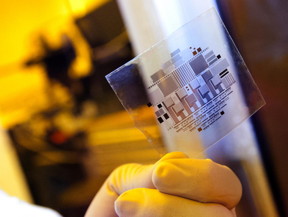 |
| A circuit made from organic thin-film transistors is fabricated on a flexible plastic substrate. A team of NIST, Wake Forest, and Penn State University researchers has identified an overlooked source of electrical resistance that can exert a dominant influence on organic-semiconductor performance. CREDIT: Patrick Mansell/Penn State |
Abstract:
It's hardly a character flaw, but organic transistors--the kind envisioned for a host of flexible electronics devices--behave less than ideally, or at least not up to the standards set by their rigid, predictable silicon counterparts. When unrecognized, a new study finds, this disparity can lead to gross overestimates of charge-carrier mobility, a property key to the performance of electronic devices.
Overlooked resistance may inflate estimates of organic-semiconductor performance: If unaccounted for, 'non-ideal' behaviors can inflate estimates of charge-carrier mobility
Gaithersburg, MD | Posted on March 13th, 2016If measurements fail to account for these divergent behaviors in so-called "organic field-effect transistors" (OFETs), the resulting estimates of how fast electrons or other charge carriers travel in the devices may be more than 10 times too high, report researchers from the National Institute of Standards and Technology (NIST), Wake Forest University and Penn State University. The team's measurements implicate an overlooked source of electrical resistance as the root of inaccuracies that can inflate estimates of organic semiconductor performance.
Their article appears in the latest issue of Nature Communications.
Already used in light-emitting diodes, or LEDs, electrically conductive polymers and small molecules are being groomed for applications in flexible displays, flat-panel TVs, sensors, "smart" textiles, solar cells and "Internet of Things" applications. Besides flexibility, a key selling point is that the organic devices--sometimes called "plastic electronics"--can be manufactured in large volumes and far more inexpensively than today's ubiquitous silicon-based devices.
A key sticking point, however, is the challenge of achieving the high levels of charge-carrier mobility that these applications require. In the semiconductor arena, the general rule is that higher mobility is always better, enabling faster, more responsive devices. So chemists have set out to hurry electrons along. Working from a large palette of organic materials, they have been searching for chemicals--alone or in combination--that will up the speed limit in their experimental devices.
Just as for silicon semiconductors, assessments of performance require measurements of current and voltage. In the basic transistor design, a source electrode injects charge into the transistor channel leading to a drain electrode. In between sits a gate electrode that regulates the current in the channel by applying voltage, functioning much like a valve.
Typically, measurements are analyzed according to a longstanding theory for silicon field-effect transistors. Plug in the current and voltage values and the theory can be used to predict properties that determine how well the transistor will perform in a circuit.
Results are rendered as a series of "transfer curves." Of particular interest in the new study are curves showing how the drain current changes in response to a change in the gate electrode voltage. For devices with ideal behavior, this relationship provides a good measure of how fast charge carriers move through the channel to the drain.
"Organic semiconductors are more prone to non-ideal behavior because the relatively weak intermolecular interactions that make them attractive for low-temperature processing also limit the ability to engineer efficient contacts as one would for state-of-the-art silicon devices," says electrical engineer David Gundlach, who leads NIST's Thin Film Electronics Project. "Since there are so many different organic materials under investigation for electronics applications, we decided to step back and do a measurement check on the conventional wisdom."
Using what Gundlach describes as the semiconductor industry's "workhorse" measurement methods, the team scrutinized an OFET made of single-crystal rubrene, an organic semiconductor with a molecule shaped a bit like a microscale insect. Their measurements revealed that electrical resistance at the source electrode--the contact point where current is injected into the OFET-- significantly influences the subsequent flow of electrons in the transistor channel, and hence the mobility.
In effect, contact resistance at the source electrode creates the equivalent of a second valve that controls the entry of current into the transistor channel. Unaccounted for in the standard theory, this valve can overwhelm the gate--the de facto� regulator between the source and drain in a silicon semiconductor transistor--and become the dominant influence on transistor behavior.
At low gate voltages, this contact resistance at the source can overwhelm device operation. Consequently, model-based estimates of charge-carrier mobility in organic semiconductors may be more than 10 times higher than the actual value, the research team reports.
Hardly ideal behavior, but the aim of the study, the researchers write, is to improve "understanding of the source of the non-ideal behavior and its impact on extracted figures of merit," especially charge-carrier mobility. This knowledge, they add, can inform efforts to develop accurate, comprehensive measurement methods for benchmarking organic semiconductor performance, as well as guide efforts to optimize contact interfaces.
####
For more information, please click here
Contacts:
Mark Bello
301-975-3776
Copyright © National Institute of Standards and Technology (NIST)
If you have a comment, please Contact us.Issuers of news releases, not 7th Wave, Inc. or Nanotechnology Now, are solely responsible for the accuracy of the content.
Bookmark:


| Related Links |
| Related News Press |
News and information
![]() Quantum computer improves AI predictions April 17th, 2026
Quantum computer improves AI predictions April 17th, 2026
![]() Flexible sensor gains sensitivity under pressure April 17th, 2026
Flexible sensor gains sensitivity under pressure April 17th, 2026
![]() A reusable chip for particulate matter sensing April 17th, 2026
A reusable chip for particulate matter sensing April 17th, 2026
![]() Detecting vibrational quantum beating in the predissociation dynamics of SF6 using time-resolved photoelectron spectroscopy April 17th, 2026
Detecting vibrational quantum beating in the predissociation dynamics of SF6 using time-resolved photoelectron spectroscopy April 17th, 2026
Organic Electronics
![]() Unveiling the power of hot carriers in plasmonic nanostructures August 16th, 2024
Unveiling the power of hot carriers in plasmonic nanostructures August 16th, 2024
Laboratories
![]() Researchers develop molecular qubits that communicate at telecom frequencies October 3rd, 2025
Researchers develop molecular qubits that communicate at telecom frequencies October 3rd, 2025
Govt.-Legislation/Regulation/Funding/Policy
![]() Quantum computer improves AI predictions April 17th, 2026
Quantum computer improves AI predictions April 17th, 2026
![]() Metasurfaces smooth light to boost magnetic sensing precision January 30th, 2026
Metasurfaces smooth light to boost magnetic sensing precision January 30th, 2026
![]() New imaging approach transforms study of bacterial biofilms August 8th, 2025
New imaging approach transforms study of bacterial biofilms August 8th, 2025
Chip Technology
![]() A reusable chip for particulate matter sensing April 17th, 2026
A reusable chip for particulate matter sensing April 17th, 2026
![]() Metasurfaces smooth light to boost magnetic sensing precision January 30th, 2026
Metasurfaces smooth light to boost magnetic sensing precision January 30th, 2026
Discoveries
![]() Quantum computer improves AI predictions April 17th, 2026
Quantum computer improves AI predictions April 17th, 2026
![]() Flexible sensor gains sensitivity under pressure April 17th, 2026
Flexible sensor gains sensitivity under pressure April 17th, 2026
![]() A reusable chip for particulate matter sensing April 17th, 2026
A reusable chip for particulate matter sensing April 17th, 2026
![]() Detecting vibrational quantum beating in the predissociation dynamics of SF6 using time-resolved photoelectron spectroscopy April 17th, 2026
Detecting vibrational quantum beating in the predissociation dynamics of SF6 using time-resolved photoelectron spectroscopy April 17th, 2026
Announcements
![]() A fundamentally new therapeutic approach to cystic fibrosis: Nanobody repairs cellular defect April 17th, 2026
A fundamentally new therapeutic approach to cystic fibrosis: Nanobody repairs cellular defect April 17th, 2026
![]() UC Irvine physicists discover method to reverse �quantum scrambling� : The work addresses the problem of information loss in quantum computing system April 17th, 2026
UC Irvine physicists discover method to reverse �quantum scrambling� : The work addresses the problem of information loss in quantum computing system April 17th, 2026
Interviews/Book Reviews/Essays/Reports/Podcasts/Journals/White papers/Posters
![]() A fundamentally new therapeutic approach to cystic fibrosis: Nanobody repairs cellular defect April 17th, 2026
A fundamentally new therapeutic approach to cystic fibrosis: Nanobody repairs cellular defect April 17th, 2026
![]() UC Irvine physicists discover method to reverse �quantum scrambling� : The work addresses the problem of information loss in quantum computing system April 17th, 2026
UC Irvine physicists discover method to reverse �quantum scrambling� : The work addresses the problem of information loss in quantum computing system April 17th, 2026
Research partnerships
![]() Lab to industry: InSe wafer-scale breakthrough for future electronics August 8th, 2025
Lab to industry: InSe wafer-scale breakthrough for future electronics August 8th, 2025
![]() HKU physicists uncover hidden order in the quantum world through deconfined quantum critical points April 25th, 2025
HKU physicists uncover hidden order in the quantum world through deconfined quantum critical points April 25th, 2025
|
|
||
|
|
||
| The latest news from around the world, FREE | ||
|
|
||
|
|
||
| Premium Products | ||
|
|
||
|
Only the news you want to read!
Learn More |
||
|
|
||
|
Full-service, expert consulting
Learn More |
||
|
|
||