Home > Press > Organic crystals allow creating flexible electronic devices: The researchers from the Faculty of Physics of the Moscow State University have grown organic crystals that allow creating flexible electronic devices
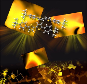 |
| The researchers from the Faculty of Physics of the Moscow State University have grown organic crystals that allow creating flexible electronic devices. CREDIT: Dmitry Yu. Paraschuk et al. |
Abstract:
Scientists from the Faculty of Physics of the Moscow State University have grown organic semiconductor crystals which can reduce the cost of the process of creating light, flexible and transparent light-emitting electronic devices of the new generation.
Organic crystals allow creating flexible electronic devices: The researchers from the Faculty of Physics of the Moscow State University have grown organic crystals that allow creating flexible electronic devices
Moscow, Russia | Posted on February 5th, 2016A team of researchers from the Faculty of Physics of Moscow State University in cooperation with Russian and foreign colleagues learnt to grow organic semiconductor crystals with extremely high light-emitting efficiency that promise a bright future for wet-processed organic optoelectronics.
Moreover, they made a double breakthrough using much simpler and cheaper technologies that previously were considered impractical. The scientists have published the results of their work in the latest issue of the Applied Materials and Interfaces journal.
The organic optoelectronics is a rapidly growing area that promises to achieve the ultimate dream to make light, flexible and transparent electronic devices of the new generation, such as organic light-emitting transistors (OLET) and organic lasers pumped by electric current. This is, indeed, a very promising area: the organic semiconductors due to their availability can even replace silicon in some electronic applications.
It was believed that the organic semiconductor crystals grown from the vapor phase are much preferred than the ones grown from solution, since those obtained from vapor are purer and free of structure impurities. A group of physicists from the Moscow State University, led by Professor Dmitry Paraschuk, are of those who do not share this opinion, and prefer the solution growing for several reasons, particularly because of much simpler and cheaper technologies stemming from this method.
In their study, so called thiophene-phenylene oligomers were chosen as work-horse molecules. The desired molecules were synthesized for them by chemists from the Moscow State University and the Enikolopov Institute of Synthetic Polymeric Materials of RAS. At the Faculty of Physics of the Moscow State University crystals were grown from solution of these molecules. Their luminescent and electrical properties were measured there as well.
The main results of this study were overwhelming: the solution-grown crystals are more luminescent than their analogues obtained from vapor. Their quantum yield (i.e. the ratio of the number of photons emitted to the number of absorbed ones) reached 60%, whereas vapor-grown crystals presented no more than 38%.
Such a striking difference in the luminescence efficiency is explained, particularly, by the fact that, perhaps, during the solution-growing some internal radiationless channels that take some part of the excitation energy are suppressed in crystals. But, apparently, this is not the only explanation.
"We have found reasons for such a high quantum yield, but we are not ready to publish these yet. This is a matter of our future studies, "- told Professor Paraschuk.
It is noteworthy that despite all previously known disadvantages of the solution-growing techniques, the new study made it possible to talk about their advantages compared to the vapor-growing methods of crystals. In one of the recent researches, the group of Paraschuk found out that crystals can be grown on the surface of the solution instead of a solid substrate, due to the surface tension forces.
"We have shown that it is possible to grow crystals on the surface of the liquid in different ways. Roughly speaking, after we place a solution with molecules in a vessel and then begin to cool it, under some certain conditions we allow molecules to be deposited on the surface at the "air-liquid" interface. Because the liquid surface is almost perfect, the crystals grown on it are of good quality, and owing to their high electronic performance they are much more preferable to the vapor-grown ones. Moreover, the surface of the solution-grown crystals is molecularly smooth with angstrom-scale roughness, which allows us to create field-effect transistors on their basis, and its quality is irreplaceable in this case" - says the professor.
Dmitry Paraschuk emphasizes that the applicability of the crystals in light-emitted transistors, and therefore in organic optoelectronics is just a suggestion, the validity of which is still to be proved. The same situation is with the possibility of creating lasers controlled by electric current obtained on the same basis.
"People dream to get lasers that can ignite by simple connection of the film to the power source, but they haven't achieved success yet,"- told Paraschuk. - "We hope that with the help of organic crystals we can reach this goal. The combination of good conductivity and high efficiency allows us to hope that the first electrically pumped laser will be created on the basis of such crystals."
####
For more information, please click here
Contacts:
Vladimir Koryagin
Copyright © Lomonosov Moscow State University
If you have a comment, please Contact us.Issuers of news releases, not 7th Wave, Inc. or Nanotechnology Now, are solely responsible for the accuracy of the content.
Bookmark:


| Related News Press |
News and information
![]() Quantum computer improves AI predictions April 17th, 2026
Quantum computer improves AI predictions April 17th, 2026
![]() Flexible sensor gains sensitivity under pressure April 17th, 2026
Flexible sensor gains sensitivity under pressure April 17th, 2026
![]() A reusable chip for particulate matter sensing April 17th, 2026
A reusable chip for particulate matter sensing April 17th, 2026
![]() Detecting vibrational quantum beating in the predissociation dynamics of SF6 using time-resolved photoelectron spectroscopy April 17th, 2026
Detecting vibrational quantum beating in the predissociation dynamics of SF6 using time-resolved photoelectron spectroscopy April 17th, 2026
Flexible Electronics
![]() Flexible sensor gains sensitivity under pressure April 17th, 2026
Flexible sensor gains sensitivity under pressure April 17th, 2026
![]() MXene nanomaterials enter a new dimension Multilayer nanomaterial: MXene flakes created at Drexel University show new promise as 1D scrolls January 30th, 2026
MXene nanomaterials enter a new dimension Multilayer nanomaterial: MXene flakes created at Drexel University show new promise as 1D scrolls January 30th, 2026
![]() Flexible electronics integrated with paper-thin structure for use in space January 17th, 2025
Flexible electronics integrated with paper-thin structure for use in space January 17th, 2025
Organic Electronics
Display technology/LEDs/SS Lighting/OLEDs
![]() Spinel-type sulfide semiconductors to operate the next-generation LEDs and solar cells For solar-cell absorbers and green-LED source October 3rd, 2025
Spinel-type sulfide semiconductors to operate the next-generation LEDs and solar cells For solar-cell absorbers and green-LED source October 3rd, 2025
Chip Technology
![]() A reusable chip for particulate matter sensing April 17th, 2026
A reusable chip for particulate matter sensing April 17th, 2026
![]() Metasurfaces smooth light to boost magnetic sensing precision January 30th, 2026
Metasurfaces smooth light to boost magnetic sensing precision January 30th, 2026
Materials/Metamaterials/Magnetoresistance
![]() First real-time observation of two-dimensional melting process: Researchers at Mainz University unveil new insights into magnetic vortex structures August 8th, 2025
First real-time observation of two-dimensional melting process: Researchers at Mainz University unveil new insights into magnetic vortex structures August 8th, 2025
![]() Researchers unveil a groundbreaking clay-based solution to capture carbon dioxide and combat climate change June 6th, 2025
Researchers unveil a groundbreaking clay-based solution to capture carbon dioxide and combat climate change June 6th, 2025
![]() A 1960s idea inspires NBI researchers to study hitherto inaccessible quantum states June 6th, 2025
A 1960s idea inspires NBI researchers to study hitherto inaccessible quantum states June 6th, 2025
![]() Institute for Nanoscience hosts annual proposal planning meeting May 16th, 2025
Institute for Nanoscience hosts annual proposal planning meeting May 16th, 2025
Announcements
![]() A fundamentally new therapeutic approach to cystic fibrosis: Nanobody repairs cellular defect April 17th, 2026
A fundamentally new therapeutic approach to cystic fibrosis: Nanobody repairs cellular defect April 17th, 2026
![]() UC Irvine physicists discover method to reverse �quantum scrambling� : The work addresses the problem of information loss in quantum computing system April 17th, 2026
UC Irvine physicists discover method to reverse �quantum scrambling� : The work addresses the problem of information loss in quantum computing system April 17th, 2026
Interviews/Book Reviews/Essays/Reports/Podcasts/Journals/White papers/Posters
![]() A fundamentally new therapeutic approach to cystic fibrosis: Nanobody repairs cellular defect April 17th, 2026
A fundamentally new therapeutic approach to cystic fibrosis: Nanobody repairs cellular defect April 17th, 2026
![]() UC Irvine physicists discover method to reverse �quantum scrambling� : The work addresses the problem of information loss in quantum computing system April 17th, 2026
UC Irvine physicists discover method to reverse �quantum scrambling� : The work addresses the problem of information loss in quantum computing system April 17th, 2026
Photonics/Optics/Lasers
![]() Metasurfaces smooth light to boost magnetic sensing precision January 30th, 2026
Metasurfaces smooth light to boost magnetic sensing precision January 30th, 2026
![]() From sensors to smart systems: the rise of AI-driven photonic noses January 30th, 2026
From sensors to smart systems: the rise of AI-driven photonic noses January 30th, 2026
|
|
||
|
|
||
| The latest news from around the world, FREE | ||
|
|
||
|
|
||
| Premium Products | ||
|
|
||
|
Only the news you want to read!
Learn More |
||
|
|
||
|
Full-service, expert consulting
Learn More |
||
|
|
||