Home > Press > Scientists have shown how to make a low-cost yet high precision glass nanoengraving: In a joint study, scientists have developed a mechanism of laser deposition of patterns on glass with a resolution of 1000 times lower than the width of a human hair
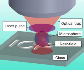 |
| This is a picture of the experimental setup. CREDIT: ACS Publications/Applied Materials & Interfaces |
Abstract:
In a joint study, scientists from the MIPT (Moscow Institute of Physics and Technology), ICP (Institute of Chemical Physics) named after Semenov, MSU (Moscow State University) and IPCP (Institute of Problems of Chemical Physics) have developed a mechanism of laser deposition of patterns on glass with a resolution of 1000 times lower than the width of a human hair. Focusing the laser was conducted with the help of small glass spheres, playing the role of the lens. This mechanism allows inexpensively and relatively easy to apply complex patterns to a glass surface, whereby obtaining a spatial resolution of less than 100 nanometers.
Scientists have shown how to make a low-cost yet high precision glass nanoengraving: In a joint study, scientists have developed a mechanism of laser deposition of patterns on glass with a resolution of 1000 times lower than the width of a human hair
Moscow, Russia | Posted on January 21st, 2016The proposed method will allow sufficiently quick and cheap creation of sensors and microchips of a nanoscale. According to the scientists, it is much cheaper and technologically easier than any of previously used methods, in addition to the fact that the new application allows deposition of the computer drawings on the glass surface with an acceptable resolution. To demonstrate this method, the abbreviation of the Institute of Chemical Physics (ICP) was deposited on glass with a high resolution (about 100 nanometers). In particular, nanoengraving is used to create ultra-precise circuits in microfluidics. The operating fluid can flow through the engraved channels connecting various parts of the circuit; and the smaller the size of such a circuit, the higher the engraving resolution.
A femtosecond laser used by scientists allows deposition of complex two-and three-dimensional patterns on the surface of transparent materials. Resolution -- the minimum size of the pattern's image detail -- is always a problem in these kinds of tasks, since it is limited (for physical reasons) by the laser wavelength. The higher the resolution, the smaller the size of patterns applied and the more interesting and sought-after these patterns in technology.
To improve the resolution, the near-field effect is often used. This method involves focusing a laser beam, using metal nanoparticles or a layer of dielectric microspheres as "lens". However, these methods complicate the pattern's deposition process, as the "lens" are fixed in space.
In their work, the authors propose a different approach: using a beam of light in fluid, they create a kind of a trap where they place glass microspheres. The advantage of this focusing method consists in that, that the "trap" can be moved, thereby moving the "lens" in space and focusing the laser to the desired area of the glass.
However, simply moving a laser beam along the surface is not enough. Exposure to laser leads to the formation of hillocks but not craters. These hillocks are quite rough and wide, but the effect of alkali at a temperature of 90� C turns the hillocks into smooth craters with a smaller width. Whereas such a two-step structuring allows achievement of a resolution below 100 nanometers (nm), one-step structuring, when the surface is treated only with a laser, does not allow obtaining precision below 150-200 nm (depending on the complexity of the structure).
As a result, the whole process of nanoengraving appears as follows. Initially, the glass surface is irradiated with a femtosecond laser. The laser pulse is focused by means of a glass bead, which is guided by an optical "trap" to a predetermined area of the glass. As a result, wide hillocks are formed on the surface of glass; but then, after surface treatment with an alkaline solution, these hillocks are converted to smaller craters of more streamlined shapes.
In addition to direct patterning process, the scientists investigated dependence of the resolution, i.e. the crater size, from the laser power. The results showed that for obtaining greater precision, it will be more effective to use small spheres, which allow obtaining a resolution below 100 nm.
The minimum width of the crater obtained was 70 nm. The figure below shows this particular crater, and the chart shows the shape of the crater on two axes.
For practical use of this method -- in addition to high resolution, you must also take into account the complexity of applying intricate structures. The above publication shows that if you use the engraving technique described, you will be able to apply relatively complex structures. To prove this, the glass surface was engraved with the abbreviation for the Institute of Chemical Physics (ICP). The average width of each letter is 100 nm, depth -- 20 nm (see Fig. below with a scale - 500 nm).
"Creating thin grooves and channels can be used in chemistry and biology fields - in the production of 'microfluidics' and at various 'nano-plants'," -- says Aleksander Shakhov, the article's co-author, post-graduate of the Faculty of General and Applied Physics at MIPT. "Channels" for liquids engraved by methods described above are used for the development of small precise sensors working with liquids. The article in question also suggests a sufficiently fast and cheap mechanism for nanostructuring. Such an approach, in particular, can allow rapid and technologically uncomplicated creation of inexpensive devices and sensors by applying complex structures of thin grooves and channels through which operating fluid will flow.
####
For more information, please click here
Contacts:
Valerii Roizen
7-929-992-2721
Copyright © Moscow Institute of Physics and Technology
If you have a comment, please Contact us.Issuers of news releases, not 7th Wave, Inc. or Nanotechnology Now, are solely responsible for the accuracy of the content.
Bookmark:


| Related Links |
| Related News Press |
News and information
![]() Quantum computer improves AI predictions April 17th, 2026
Quantum computer improves AI predictions April 17th, 2026
![]() Flexible sensor gains sensitivity under pressure April 17th, 2026
Flexible sensor gains sensitivity under pressure April 17th, 2026
![]() A reusable chip for particulate matter sensing April 17th, 2026
A reusable chip for particulate matter sensing April 17th, 2026
![]() Detecting vibrational quantum beating in the predissociation dynamics of SF6 using time-resolved photoelectron spectroscopy April 17th, 2026
Detecting vibrational quantum beating in the predissociation dynamics of SF6 using time-resolved photoelectron spectroscopy April 17th, 2026
Chemistry
![]() Projecting light to dispense liquids: A new route to ultra-precise microdroplets January 30th, 2026
Projecting light to dispense liquids: A new route to ultra-precise microdroplets January 30th, 2026
![]() From sensors to smart systems: the rise of AI-driven photonic noses January 30th, 2026
From sensors to smart systems: the rise of AI-driven photonic noses January 30th, 2026
![]() "Nanoreactor" cage uses visible light for catalytic and ultra-selective cross-cycloadditions October 3rd, 2025
"Nanoreactor" cage uses visible light for catalytic and ultra-selective cross-cycloadditions October 3rd, 2025
![]() Cambridge chemists discover simple way to build bigger molecules � one carbon at a time June 6th, 2025
Cambridge chemists discover simple way to build bigger molecules � one carbon at a time June 6th, 2025
Microfluidics/Nanofluidics
![]() Projecting light to dispense liquids: A new route to ultra-precise microdroplets January 30th, 2026
Projecting light to dispense liquids: A new route to ultra-precise microdroplets January 30th, 2026
Possible Futures
![]() A fundamentally new therapeutic approach to cystic fibrosis: Nanobody repairs cellular defect April 17th, 2026
A fundamentally new therapeutic approach to cystic fibrosis: Nanobody repairs cellular defect April 17th, 2026
![]() UC Irvine physicists discover method to reverse �quantum scrambling� : The work addresses the problem of information loss in quantum computing system April 17th, 2026
UC Irvine physicists discover method to reverse �quantum scrambling� : The work addresses the problem of information loss in quantum computing system April 17th, 2026
Chip Technology
![]() A reusable chip for particulate matter sensing April 17th, 2026
A reusable chip for particulate matter sensing April 17th, 2026
![]() Metasurfaces smooth light to boost magnetic sensing precision January 30th, 2026
Metasurfaces smooth light to boost magnetic sensing precision January 30th, 2026
Sensors
![]() Flexible sensor gains sensitivity under pressure April 17th, 2026
Flexible sensor gains sensitivity under pressure April 17th, 2026
![]() Tiny nanosheets, big leap: A new sensor detects ethanol at ultra-low levels January 30th, 2026
Tiny nanosheets, big leap: A new sensor detects ethanol at ultra-low levels January 30th, 2026
![]() From sensors to smart systems: the rise of AI-driven photonic noses January 30th, 2026
From sensors to smart systems: the rise of AI-driven photonic noses January 30th, 2026
![]() Sensors innovations for smart lithium-based batteries: advancements, opportunities, and potential challenges August 8th, 2025
Sensors innovations for smart lithium-based batteries: advancements, opportunities, and potential challenges August 8th, 2025
Discoveries
![]() Quantum computer improves AI predictions April 17th, 2026
Quantum computer improves AI predictions April 17th, 2026
![]() Flexible sensor gains sensitivity under pressure April 17th, 2026
Flexible sensor gains sensitivity under pressure April 17th, 2026
![]() A reusable chip for particulate matter sensing April 17th, 2026
A reusable chip for particulate matter sensing April 17th, 2026
![]() Detecting vibrational quantum beating in the predissociation dynamics of SF6 using time-resolved photoelectron spectroscopy April 17th, 2026
Detecting vibrational quantum beating in the predissociation dynamics of SF6 using time-resolved photoelectron spectroscopy April 17th, 2026
Announcements
![]() A fundamentally new therapeutic approach to cystic fibrosis: Nanobody repairs cellular defect April 17th, 2026
A fundamentally new therapeutic approach to cystic fibrosis: Nanobody repairs cellular defect April 17th, 2026
![]() UC Irvine physicists discover method to reverse �quantum scrambling� : The work addresses the problem of information loss in quantum computing system April 17th, 2026
UC Irvine physicists discover method to reverse �quantum scrambling� : The work addresses the problem of information loss in quantum computing system April 17th, 2026
Interviews/Book Reviews/Essays/Reports/Podcasts/Journals/White papers/Posters
![]() A fundamentally new therapeutic approach to cystic fibrosis: Nanobody repairs cellular defect April 17th, 2026
A fundamentally new therapeutic approach to cystic fibrosis: Nanobody repairs cellular defect April 17th, 2026
![]() UC Irvine physicists discover method to reverse �quantum scrambling� : The work addresses the problem of information loss in quantum computing system April 17th, 2026
UC Irvine physicists discover method to reverse �quantum scrambling� : The work addresses the problem of information loss in quantum computing system April 17th, 2026
Tools
![]() Metasurfaces smooth light to boost magnetic sensing precision January 30th, 2026
Metasurfaces smooth light to boost magnetic sensing precision January 30th, 2026
![]() From sensors to smart systems: the rise of AI-driven photonic noses January 30th, 2026
From sensors to smart systems: the rise of AI-driven photonic noses January 30th, 2026
![]() Japan launches fully domestically produced quantum computer: Expo visitors to experience quantum computing firsthand August 8th, 2025
Japan launches fully domestically produced quantum computer: Expo visitors to experience quantum computing firsthand August 8th, 2025
Photonics/Optics/Lasers
![]() Metasurfaces smooth light to boost magnetic sensing precision January 30th, 2026
Metasurfaces smooth light to boost magnetic sensing precision January 30th, 2026
![]() From sensors to smart systems: the rise of AI-driven photonic noses January 30th, 2026
From sensors to smart systems: the rise of AI-driven photonic noses January 30th, 2026
Research partnerships
![]() Lab to industry: InSe wafer-scale breakthrough for future electronics August 8th, 2025
Lab to industry: InSe wafer-scale breakthrough for future electronics August 8th, 2025
![]() HKU physicists uncover hidden order in the quantum world through deconfined quantum critical points April 25th, 2025
HKU physicists uncover hidden order in the quantum world through deconfined quantum critical points April 25th, 2025
|
|
||
|
|
||
| The latest news from around the world, FREE | ||
|
|
||
|
|
||
| Premium Products | ||
|
|
||
|
Only the news you want to read!
Learn More |
||
|
|
||
|
Full-service, expert consulting
Learn More |
||
|
|
||